


MPC563XM Reference Manual, Rev. 1
272
Freescale Semiconductor
Preliminary—Subject to Change Without Notice
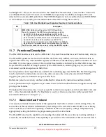
User Test 0 register (CFLASH_UT0)
Address Offset: 0x0003C
Reset value: 0x00000001
10-14
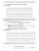
BK1_RWSC
Bank1 Read Wait State Control. This field is used to control the number of wait-states to be
added to the Flash array access time for reads. This field must be set to a value corresponding to
the operating frequency of the PFLASH and the actual read access time of the PFLASH. The
required settings are documented in the SoC specification. Higher operating frequencies require
non-zero settings for this field for proper Flash operation.
Shown below are the maximum operating frequencies for legal APC and RWSC settings based
on estimated ST LC Flash access times at 150°C. The integrator is strongly encouraged to verify
these settings based on actual silicon results.
0 MHz, < 23 MHz
APC=RWSC=0
23 MHz, < 45 MHz
APC=RWSC=1
45 MHz, < 68 MHz
APC=RWSC=2
68 MHz, < 90 MHz
APC=RWSC=3
00000
No additional wait-states are added
00001
1 additional wait-state is added
00010
2 additional wait-states are added
...
111111 31 additional wait-states are added
This field is ignored in single bank Flash configurations.
15-16, 24
BK1_RWWC
Bank1 Read-While-Write Control. This 3-bit field defines the controller response to Flash reads
while the array is busy with a program (write) or erase operation.
0--
Terminate any attempted read-while-write/erase with an error response
111 Generate a bus stall for a read-while-write/erase, disable the stall notification interrupt,
disable the abort + abort notification interrupt
110 Generate a bus stall for a read-while-write/erase, enable the stall notification interrupt,
disable the abort + abort notification interrupt
101 Generate a bus stall for a read-while-write/erase, enable the operation abort, disable
the abort notification interrupt
100 Generate a bus stall for a read-while-write/erase, enable the operation abort and the abort
notification interrupt
This field is set to 0b111 by hardware reset enabling the stall-while-write/erase and disabling the
abort and notification interrupts.
17-23, 25-30
Reserved, should be cleared.
31
B1_P0_BFE
Bank1, Port 0 Buffer Enable. This bit enables or disables read hits from the 128-bit holding
register. It is also used to invalidate the contents of the holding register. This bit is set by hardware
reset, enabling the use of the holding register.
0
The holding register is disabled from satisfying read requests.
1
The holding register is enabled to satisfy read requests on hits.
0
1
2
3
4
5
6
7
8
9
10
11
12
13
14
15
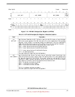
UTE
0
0
0
0
0
0
0
DSI7 DSI6 DSI5 DSI4 DSI3 DSI2 DSI1 DSI0
rw/0
r/0
r/0
r/0
r/0
r/0
r/0
r/0
rw/0
rw/0
rw/0
rw/0
rw/0
rw/0
rw/0
rw/0
Table 11-18. PFLASH Configuration Register 3 Field Descriptions (continued)
Field
Description


