


MPC563XM Reference Manual, Rev. 1
Freescale Semiconductor
1193
Preliminary—Subject to Change Without Notice
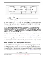
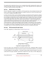
Figure 26-29. Peripheral Chip Select Strobe Timing
The delay between the assertion of the PCS signals and the assertion of PCSS is selected by the PCSSCK
field in the DSPI_CTAR based on the following formula:
Eqn. 26-5
At the end of the transfer the delay between PCSS negation and PCS negation is selected by the PASC field
in the DSPI_CTAR based on the following formula:
Eqn. 26-6
shows an example of how to compute the t
pcssck
delay.
shows an example of how to compute the t
pasc
delay.
The PCSS signal is not supported when Continuous Serial Communication SCK is enabled
(CONT_SCKE=1).
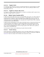
26.5.7
Transfer Formats
The SPI serial communication is controlled by the Serial Communications Clock (SCK) signal and the
PCS signals. The SCK signal provided by the Master device synchronizes shifting and sampling of the data
on the SIN and SOUT pins. The PCS signals serve as enable signals for the slave devices.
When the DSPI is the bus master, the CPOL and CPHA bits in the DSPI Clock and Transfer Attributes
Registers (DSPI_CTARx) select the polarity and phase of the serial clock, SCK. The polarity bit selects
the idle state of the SCK. The clock phase bit selects if the data on SOUT is valid before or on the first
SCK edge.
When the DSPI is the bus Slave, CPOL and CPHA bits in the DSPI_CTAR0 (SPI) or DSPI_CTAR1 (DSI)
select the polarity and phase of the serial clock. For SPI Slaves the DSPI_CTAR0 is used, and for DSI
Table 26-39. Peripheral Chip Select Strobe Assert Computation Example
PCSSCK
Prescaler
f
sys
Delay before Transfer
0b11
7
100 MHz
70.0 ns
Table 26-40. Peripheral Chip Select Strobe Negate Computation Example
PASC
Prescaler
f
sys
Delay after Transfer
0b11
7
100 MHz
70.0 ns
t
PCSSCK
PCSS
PCSx
t
PASC
t
PCSSCK
1
f
SYS
----------
PCSSCK
×
=
t
PASC
1
f
SYS
----------
PASC
×
=


