


MPC563XM Reference Manual, Rev. 1
1006
Freescale Semiconductor
Preliminary—Subject to Change Without Notice
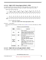
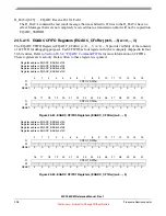
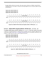
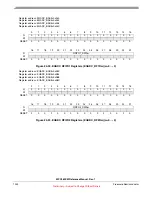
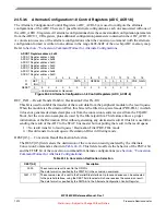
24.5.3.1
ADC0/1 Control Registers (ADC0_CR and ADC1_CR)
The ADC0/1 Control Registers (ADC0/1_CR) is used to define the standard configuration of the ADC. In
the standard configuration, the parameters contained in the Alternate Configuration Control Registers
(ADC_ACR1-8) are fixed at their reset value. A conversion uses the standard configuration when the
conversion command (with the standard format) is written to address 0x00 of the on-chip ADC memory
map. Refer to
Section , “Conversion Command Format for the Standard Configuration
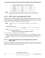
0x42
Reserved
-
0x43
Reserved
-
0x44
Alternate Configuration 6 Control Register (ADC_ACR6)
Write/Read
0x45
Reserved
-
0x46
Reserved
-
0x47
Reserved
-
0x48
Alternate Configuration 7 Control Register (ADC_ACR7)
Write/Read
0x49
Reserved
-
0x4A
Reserved
-
0x4B
Reserved
-
0x4C
Alternate Configuration 8 Control Register (ADC_ACR8)
Write/Read
0x4D-0x6F
Reserved
-
0x70
Pull Up/Down Control Register0 (ADC_PUDCR0)
Write/Read
0x71
Pull Up/Down Control Register0 (ADC_PUDCR1)
Write/Read
0x72
Pull Up/Down Control Register0 (ADC_PUDCR2)
Write/Read
0x73
Pull Up/Down Control Register0 (ADC_PUDCR3)
Write/Read
0x74
Pull Up/Down Control Register0 (ADC_PUDCR4)
Write/Read
0x75
Pull Up/Down Control Register0 (ADC_PUDCR5)
Write/Read
0x76
Pull Up/Down Control Register0 (ADC_PUDCR6)
Write/Read
0x77
Pull Up/Down Control Register0 (ADC_PUDCR7)
Write/Read
0x78-0x97
Reserved for ADC_PUDCR8 to ADC_PUDCR39
-
0x98-0xFF
Reserved
-
1
Throughout the table, ADC0/ADC1 indicates that if the command is stored in CBuffer0 it will be applied to
ADC0 and if in CBuffer1 it applies to ADC1. If this indication is omitted the register applies for both ADC0 and
ADC1, independent of the CBuffer used.
Table 24-13. On-Chip ADC Memory Map (continued)


