


ADSP-BF59x Blackfin Processor Hardware Reference
15-3
Parallel Peripheral Interface
Interface Overview
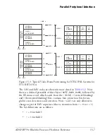
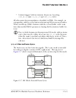
Figure 15-1
shows a block diagram of the PPI.
The
PPI_CLK
pin accepts an external clock input. It cannot source a clock
internally.
When the
PPI_CLK
is not free-running, there may be additional
latency cycles before data gets received or transmitted. In RX and
TX modes, there may be at least 2 cycles latency before valid data is
received or transmitted.
The
PPI_CLK
not only supplies the PPI module itself, but it also can clock
one or more GP Timers to work synchronously with the PPI. Depending
on PPI operation mode, the
PPI_CLK
can either equal or invert the
TMRCLK
input. For more information, see
Chapter 8, “General-Purpose Timers”
.
Figure 15-1. PPI Block Diagram
DATA BUS
PPI_CLK
16 BITS
*
16-DEEP
FIFO
FS1
PPI_CONTROL
PACK/
UNPACK
PPI_COUNT
PPI_STATUS
PPI_DELAY
PPI_FRAME
GATE
SYNC
FS2
FS3
DMA
CONTROLLER
PAB
DAB
Summary of Contents for ADSP-BF59x Blackfin
Page 64: ...Development Tools 1 22 ADSP BF59x Blackfin Processor Hardware Reference...
Page 74: ...Processor Specific MMRs 2 10 ADSP BF59x Blackfin Processor Hardware Reference...
Page 244: ...Programming Examples 6 40 ADSP BF59x Blackfin Processor Hardware Reference...
Page 700: ...Programming Examples 16 78 ADSP BF59x Blackfin Processor Hardware Reference...
Page 738: ...Boundary Scan Architecture B 8 ADSP BF59x Blackfin Processor Hardware Reference...