


ADSP-BF59x Blackfin Processor Hardware Reference
1-5
Introduction
and larger, lower cost and lower performance off-chip memory systems.
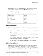
Table 1-2
shows the memory for the ADSP-BF59x processors.
Internal Memory
The processor has four blocks of on-chip memory that provide high band-
width access to the core:
• L1 instruction SRAM memory. This memory is accessed at full
processor speed.
• L1 data SRAM memory. This memory block is accessed at full pro-
cessor speed.
• L1 scratchpad RAM, which runs at the same speed as the L1 mem-
ories but is only accessible as data SRAM.
• L1 instruction ROM memory, accessed at full processor speed.
I/O Memory Space
Blackfin processors do not define a separate I/O space. All resources are
mapped through the flat 32-bit address space. Control registers for
on-chip I/O devices are mapped into memory-mapped registers (MMRs)
at addresses near the top of the 4G byte address space. These are separated
Table 1-2. Memory Configurations
Type of Memory
ADSP-BF59x
Instruction SRAM
32K byte
Instruction ROM
64K byte
Data SRAM
32K byte
Data scratchpad SRAM
4K byte
L3 Boot ROM
4K byte
Total
136K byte
Summary of Contents for ADSP-BF59x Blackfin
Page 64: ...Development Tools 1 22 ADSP BF59x Blackfin Processor Hardware Reference...
Page 74: ...Processor Specific MMRs 2 10 ADSP BF59x Blackfin Processor Hardware Reference...
Page 244: ...Programming Examples 6 40 ADSP BF59x Blackfin Processor Hardware Reference...
Page 700: ...Programming Examples 16 78 ADSP BF59x Blackfin Processor Hardware Reference...
Page 738: ...Boundary Scan Architecture B 8 ADSP BF59x Blackfin Processor Hardware Reference...