


Unique Information for the ADSP-BF59x Processor
8-58
ADSP-BF59x Blackfin Processor Hardware Reference
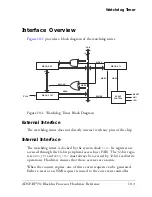
External Interface
The
TMRCLK
input is common to all three timers. The PPI unit is clocked
by the same pin; therefore any of the timers can be clocked by
PPI_CLK
.
Since timer 0 and timer 1 are often used in conjunction with the PPI, they
are internally looped back to the PPI module for frame sync generation.
The timer signals
TMR0
and
TMR1
are multiplexed with the PPI frame syncs
when the frame syncs are applied externally. PPI modes requiring only one
frame sync free up
TMR1
. For details, see the
Parallel Peripheral Interface
chapter.
If the PPI frame syncs are applied externally, timer 0 and timer 1
are still fully functional and can be used for other purposes not
involving the
TMRx
pins. Timer 0 and timer 1 must not drive their
TMR0
and
TMR1
pins. If operating in
PWM_OUT
mode, the
OUT_DIS
bit
in the
TIMER0_CONFIG
and
TIMER1_CONFIG
registers must be set.
Summary of Contents for ADSP-BF59x Blackfin
Page 64: ...Development Tools 1 22 ADSP BF59x Blackfin Processor Hardware Reference...
Page 74: ...Processor Specific MMRs 2 10 ADSP BF59x Blackfin Processor Hardware Reference...
Page 244: ...Programming Examples 6 40 ADSP BF59x Blackfin Processor Hardware Reference...
Page 700: ...Programming Examples 16 78 ADSP BF59x Blackfin Processor Hardware Reference...
Page 738: ...Boundary Scan Architecture B 8 ADSP BF59x Blackfin Processor Hardware Reference...