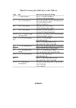
Main Revisions and Additions in this Edition
Page
Item
Revisions (See Manual for Details)
6
1.2 Block Diagram
Figure 1.1 Internal Block Diagram
PLLVCC and PLLVSS pins added
151
4.5.12 Burst Operation
Figure 4.29 Operation Timing in Fast Page Mode (1)
Title in parentheses amended
CAST = 1
→
CAST = 0
286
5.16.3 Pin Functions
Table 5.35 Port G Pin Functions
PG3 to PG0: Description amended
291
5.17.3 Pin Functions
Table 5.37 Port H Pin Functions
PH1 and PH0: Description amended
295, 296 5.18.1 Port States in Each
Processing State
Table 5.38 I/O Port States in Each Processing State
PG5 and PG4 states amended
378 to
380
7.1.2 DC Characteristics
Table 7.2 DC Characteristics
Entire table amended
Table 7.3 Permissible Output Currents
Max. values of
Σ
I
OL
and
Σ
–I
OH
amended
384
7.1.3 AC Characteristics
Figure 7.3 (2) Oscillation Stabilization Timing added
414
Figure 7.36 WDT Output Timing amended
417
7.2.1 Absolute Maximum
Ratings
Table 7.11 Absolute Maximum Ratings
Note: Operating temperature ranges amended
418, 419 7.2.2 DC Characteristics
Table 7.12 DC Characteristics
Entire table amended
420
Table 7.13 Permissible Output Currents
Max. values of
Σ
I
OL
and
Σ
–I
OH
amended
432, 433 7.2.6 Flash Memory
Characteristics
Conditions: Operating temperature range amended
Unit of t
E
amended
z and
γ
amended
Summary of Contents for H8S/2670
Page 5: ......
Page 9: ......
Page 199: ...182 ...
Page 361: ...344 ...
Page 393: ...376 ...
Page 647: ...630 ...


