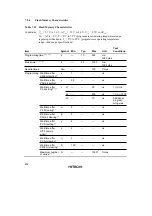


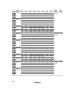
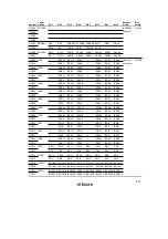
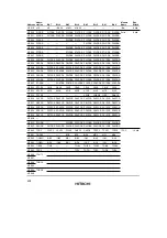
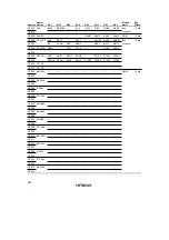
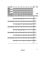
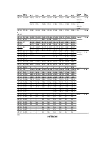
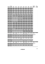
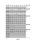

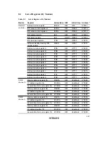
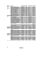
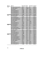
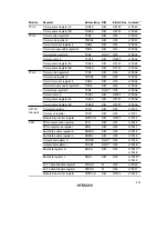
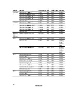
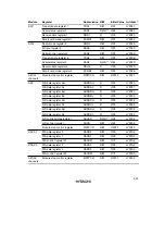
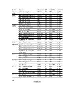
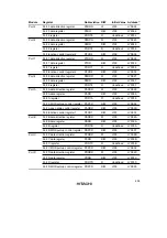
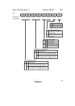


446
Address
Abbre-
viation
Bit 7
Bit 6
Bit 5
Bit 4
Bit 3
Bit 2
Bit 1
Bit 0
Module
Name
Bus
Width
H'FFF0
TCR2
—
CCLR1
CCLR0
CKEG1
CKEG0
TPSC2
TPSC1
TPSC0
TPU2
16 bits
H'FFF1
TMDR2
—
—
—
—
MD3
MD2
MD1
MD0
H'FFF2
TIOR2
IOB3
IOB2
IOB1
IOB0
IOA3
IOA2
IOA1
IOA0
H'FFF4
TIER2
TTGE
—
TCIEU
TCIEV
—
—
TGIEB
TGIEA
H'FFF5
TSR2
TCFD
—
TCFU
TCFV
—
—
TGFB
TGFA
H'FFF6
TCNT2
H'FFF7
H'FFF8
TGR2A
H'FFF9
H'FFFA
TGR2B
H'FFFB
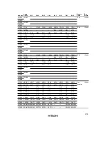
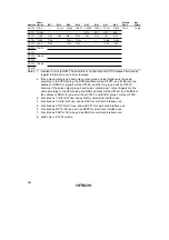
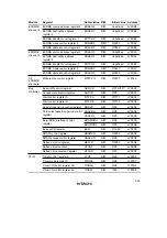
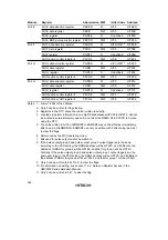
Notes: 1. Located in on-chip RAM. The bus width is 32 bits when the DTC accesses this area as
register information, and 16 bits otherwise.
2. If the pulse output group 2 and pulse output group 3 output triggers are the same
according to the PCR setting, the NDRH address will be H'FF4C, and if different, the
address of NDRH for group 2 will be H'FF4E, and that for group 3 will be H'FF4C.
Similarly, if the pulse output group 0 and pulse output group 1 output triggers are the
same according to the PCR setting, the NDRL address will be H'FF4D, and if different,
the address of NDRL for group 0 will be H'FF4F, and that for group 1 will be H'FF4D.
3. Functions as C/
A
for SCI use, and as GM for smart card interface use.
4. Functions as CHR for SCI use, and as BLK for smart card interface use.
5. Functions as STOP for SCI use, and as BCP1 for smart card interface use.
6. Functions as MP for SCI use, and as BCP0 for smart card interface use.
7. Functions as FER for SCI use, and as ERS for smart card interface use.
8. Valid only in F-ZTAT version
Summary of Contents for H8S/2670
Page 5: ......
Page 9: ......
Page 199: ...182 ...
Page 361: ...344 ...
Page 393: ...376 ...
Page 647: ...630 ...