556
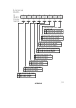
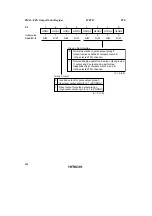
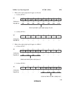
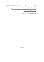
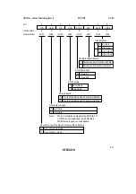
PMR—PPG Output Mode Register
H'FF47
PPG
Bit
Initial value
Read/Write
7
G3INV
1
R/W
6
G2INV
1
R/W
5
G1INV
1
R/W
4
G0INV
1
R/W
3
G3NOV
0
R/W
2
G2NOV
0
R/W
1
G1NOV
0
R/W
0
G0NOV
0
R/W
Group n Non-Overlap
0
Normal operation in pulse output group 0
(output values updated at compare match A
in the selected TPU channel)
1
Non-overlapping operation in pulse output group n
(1 output and 0 output can be performed
independently at compare match A and B
in the selected TPU channel)
(n = 3 to 0)
Group n Invert
0
Inverted output for pulse output group n
(low-level output at pin for a 1 in PODRH)
1
Direct output for pulse output group n
(high-level output at pin for a 1 in PODRH)
(n = 3 to 0)
Summary of Contents for H8S/2670
Page 5: ......
Page 9: ......
Page 199: ...182 ...
Page 361: ...344 ...
Page 393: ...376 ...
Page 647: ...630 ...


