166
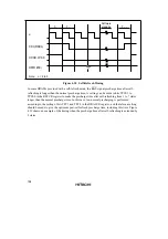
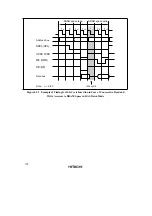
Write after Read: If an external write occurs after an external read while the ICIS0 bit is set to 1
in the BCR register, an idle cycle is inserted at the start of the write cycle.
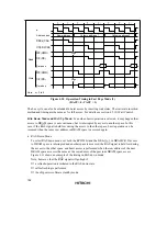
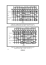
Figure 4.45 shows an example of the operation in this case. In this example, bus cycle A is a read
cycle for ROM with a long output floating time, and bus cycle B is a CPU write cycle. In (a), an
idle cycle is not inserted, and a collision occurs in bus cycle B between the read data from ROM
and the CPU write data. In (b), an idle cycle is inserted, and a data collision is prevented.
T
1
Address bus
ø
RD
Bus cycle A
Data bus
T
2
T
3
T
1
T
2
Bus cycle B
Long output
floating time
Data
collision
(a) Idle cycle not inserted
(ICIS0 = 0)
T
1
Address bus
ø
RD
Bus cycle A
Data bus
T
2
T
3
T
i
T
1
Bus cycle B
(b) Idle cycle inserted
(ICIS0 = 1 (initial value))
T
2
HWR
HWR
CS
(area A)
CS
(area B)
CS
(area A)
CS
(area B)
;
y
Figure 4.45 Example of Idle Cycle Operation (2) (Write after Read)
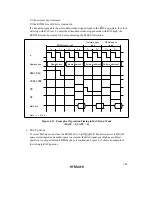
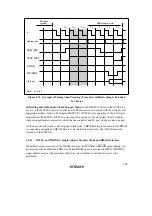
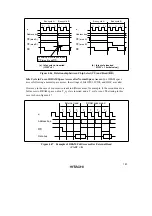
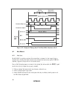
Relationship between Chip Select (
CS
) Signal and Read (
RD
) Signal: Depending on the
system’s load conditions, the
RD
signal may lag behind the
CS
signal. An example is shown in
figure 4.46.
In this case, with the setting for no idle cycle insertion (a), there may be a period of overlap
between the bus cycle A
RD
signal and the bus cycle B
CS
signal.
Setting idle cycle insertion, as in (b), however, will prevent any overlap between the
RD
and
CS
signals.
In the initial state after reset release, idle cycle insertion (b) is set.
Summary of Contents for H8S/2670
Page 5: ......
Page 9: ......
Page 199: ...182 ...
Page 361: ...344 ...
Page 393: ...376 ...
Page 647: ...630 ...

