107
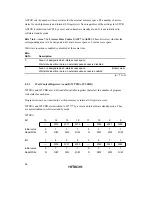
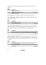
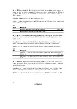
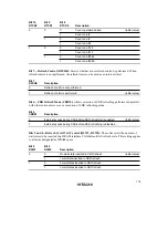
Bit 9—Write Data Buffer Enable (WDBE): Selects whether or not the write data buffer function
is used for an external write cycle or DMAC single address transfer cycle.
Bit 9
WDBE
Description
0
Write data buffer function not used
(Initial value)
1
Write data buffer function used
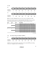
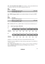
Bit 8—
WAIT
Pin Enable (WAITE): Selects enabling or disabling of wait input by the
WAIT
pin.
Bit 8
WAITE
Description
0
Wait input by
WAIT
pin disabled
WAIT
pin can be used as I/O port
(Initial value)
1
Wait input by
WAIT
pin enabled
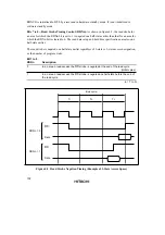
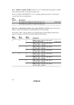
Bits 7 to 0—Reserved: These are readable/writable bits, but the write value should always be 0.
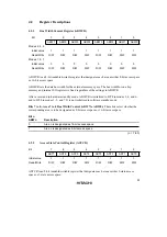
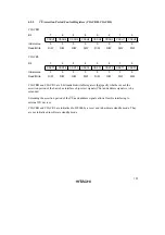
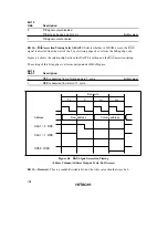
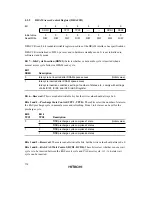
4.2.8
DRAM Control Register (DRAMCR)
Bit
15
14
13
12
11
10
9
8
OEE
RAST
—
CAST
—
RMTS2
RMTS1
RMTS0
Initial value
0
0
0
0
0
0
0
0
Read/Write
R/W
R/W
R/W
R/W
R/W
R/W
R/W
R/W
Bit
7
6
5
4
3
2
1
0
BE
RCDM
DDS
EDDS
—
MXC2
MXC1
MXC0
Initial value
0
0
0
0
0
0
0
0
Read/Write
R/W
R/W
R/W
R/W
R/W
R/W
R/W
R/W
DRAMCR is a 16-bit readable/writable register used to make DRAM interface settings.
DRAMCR is initialized to H'0000 by a reset and in hardware standby mode. It is not initialized in
software standby mode.
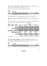
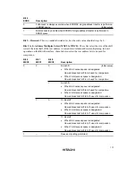
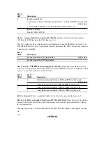
Bit 15—
OE
Output Enable (OEE): Enables or disables output from the
OE
pin of the
OE
signal
used when EDO page mode DRAM is connected. The
OE
signal is common to all areas
designated as DRAM space.
Summary of Contents for H8S/2670
Page 5: ......
Page 9: ......
Page 199: ...182 ...
Page 361: ...344 ...
Page 393: ...376 ...
Page 647: ...630 ...


