315
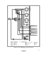
Reset
WDDR6
Reset
WDR6
P6n
RDR6
RPFCR2
RPOR6
Reset
WPFCR2
DMA controller
*
DMA transfer acknowledge
enable
DMA transfer acknowledge
8-bit timer module
Compare match output
enable
Compare match output
Interrupt controller
ITSm
IRQm
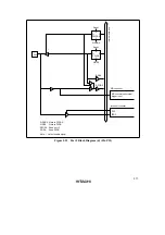
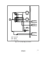
WDDR6: Write to P6DDR
WDR6:
Write to P6DR
WPFCR2: Write to PFCR2
RPOR6:
Read port 6
RDR6: Read
P6DR
RPFCR2: Read PFCR2
n = 4 or 5
m = 12 or 13
R
P6nDDR
C
Q
D
R
P6nDR
C
Q
D
R
Q
D
C
DMACS
PFCR2
Internal data bus
Note:
*
Output enable signal
Priority order: DMACS = 0
DMAC
>
TMR
>
DR
DMACS = 1
TMR
>
DR
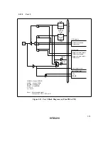
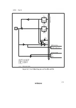
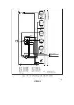
Figure 5.37 Port 6 Block Diagram (c) (Pins P64 and P65)
Summary of Contents for H8S/2670
Page 5: ......
Page 9: ......
Page 199: ...182 ...
Page 361: ...344 ...
Page 393: ...376 ...
Page 647: ...630 ...

