541
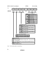
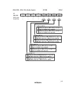
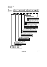
Short address mode
Bit
DMACR
Initial value
Read/Write
7
DTSZ
0
R/W
6
DTID
0
R/W
5
RPE
0
R/W
4
DTDIR
0
R/W
3
DTF3
0
R/W
2
DTF2
0
R/W
1
DTF1
0
R/W
0
DTF0
0
R/W
Data Transfer Factor
0
—
Channel A
Channel B
1
0
1
Activated by A/D converter conversion
end interrupt
—
—
Activated by
DREQ
pin
falling edge input
Activated by
DREQ
pin
low-level input
Activated by SCI channel 0 transmission
complete interrupt
Activated by SCI channel 0 reception
complete interrupt
0
1
0
1
0
0
1
Activated by SCI channel 1 transmission
complete interrupt
1
0
Activated by SCI channel 1 reception
complete interrupt
1
0
0
1
Activated by TPU channel 0 compare match/
input capture A interrupt
1
0
1
Activated by TPU channel 1 compare match/
input capture A interrupt
Activated by TPU channel 2 compare match/
input capture A interrupt
Activated by TPU channel 3 compare match/
input capture A interrupt
Activated by TPU channel 4 compare match/
input capture A interrupt
Activated by TPU channel 5 compare match/
input capture A interrupt
0
1
0
1
0
0
1
—
1
0
—
1
Data Transfer Direction
0
Dual address mode: Transfer with MAR as source address and IOAR as destination address
Single address mode: Transfer with MAR as source address and
DACK
pin as write strobe
1
Dual address mode: Transfer with IOAR as source address and MAR as destination address
Single address mode: Transfer with
DACK
as read strobe and MAR as destination address
Repeat Enable
0
Sequential mode
1
Repeat mode or idle mode
Data Transfer Increment/
Decrement
0
MAR is incremented
after a data transfer
1
MAR is decremented
after a data transfer
Data Transfer Size
0
Byte-size transfer
1
Word-size transfer
Summary of Contents for H8S/2670
Page 5: ......
Page 9: ......
Page 199: ...182 ...
Page 361: ...344 ...
Page 393: ...376 ...
Page 647: ...630 ...


