197
Pin
Selection Method and Pin Functions
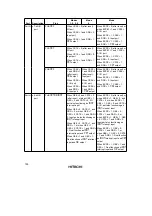
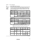
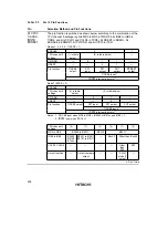
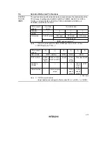
P15/PO13/
TIOCB1/
TCLKC
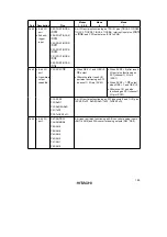
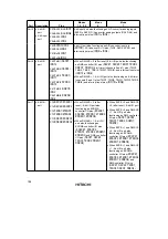
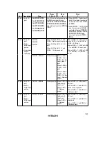
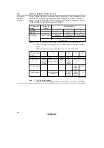
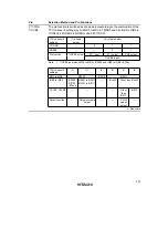
The pin function is switched as shown below according to the combination of the
TPU channel 1 settings (by bits MD3 to MD0 in TMDR1, bits IOB3 to IOB0 in
TIOR1, and bits CCLR1 and CCLR0 in TCR1), bits TPSC2 to TPSC0 in TCR0,
TCR2, TCR4, and TCR5, bit NDER13 in NDERH, and bit P15DDR.
TPU channel 1
settings
(1) in table
below
(2) in table below
P15DDR
—
0
1
1
NDER13
—
—
0
1
Pin function
TIOCB1 output
P15 input
P15 output
PO13 output
TIOCB1 input
*
1
TCLKC input
*
2
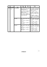
Notes: 1. TIOCB1 input when MD3 to MD0 = B'0000 or B'01XX and IOB3 to IOB0 =
B'10xx.
2. TCLKC input when the setting for either TCR0 or TCR2 is TPSC2 to TPSC0 =
B'110, or when the setting for either TCR4 or TCR5 is TPSC2 to TPSC0 =
B'101.
TCLKC input when phase counting mode is set for channels 2 and 4.
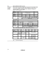
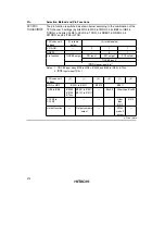
TPU channel 1
settings
(2)
(1)
(2)
(2)
(1)
(2)
MD3 to MD0
B'0000, B'01xx
B'0010
B'0011
IOB3 to IOB0
B'0000
B'0100
B'1xxx
B'0001 to B'0011
B'0101 to B'0111
—
B'xx00
Other than B'xx00
CCLR1, CCLR0
—
—
—
—
Other
than
B'10
B'10
Output function
—
Output compare
output
—
—
PWM
mode 2
output
—
x: Don’t care
Summary of Contents for H8S/2670
Page 5: ......
Page 9: ......
Page 199: ...182 ...
Page 361: ...344 ...
Page 393: ...376 ...
Page 647: ...630 ...

