137
4.4.7
Extension of Chip Select (
CS
) Assertion Period
Some external I/O devices require a setup time and hold time between address and
CS
signals and
strobe signals such as
RD
,
HWR
, and
LWR
. Settings can be made in the CSACR register to insert
states in which only the
CS
,
AS
, and address signals are asserted before and after a basic bus space
access cycle. Extension of the
CS
assertion period can be set for individual areas.
With the
CS
assertion extension period in write access, the data setup and hold times are less
stringent since the write data is output to the data bus.
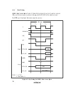
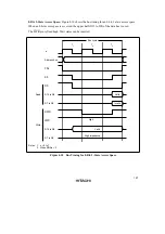
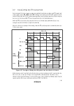
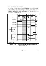
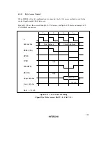
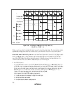
Figure 4.19 shows an example of the timing when the
CS
assertion period is extended in basic bus
3-state access space.
T
h
Address bus
ø
T
1
T
2
T
3
T
t
Bus cycle
Data bus
HWR
,
LWR
Write
Data bus
RD
CSn
AS
Read
(when
RDNn = 0)
Read data
Write data
Figure 4.19 Example of Timing when Chip Select Assertion Period is Extended
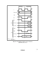
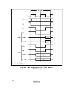
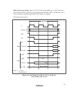
Both extension state T
h
inserted before the basic bus cycle and extension state T
t
inserted after the
basic bus cycle, or only one of these, can be specified for individual areas. Insertion or non-
insertion can be specified for the T
h
state with the upper 8 bits (CSXH7 to CSXH0) in the CSACR
register, and for the T
t
state with the lower 8 bits (CSXT7 to CSXT0).
Summary of Contents for H8S/2670
Page 5: ......
Page 9: ......
Page 199: ...182 ...
Page 361: ...344 ...
Page 393: ...376 ...
Page 647: ...630 ...

