410
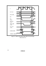
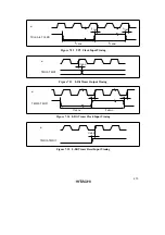
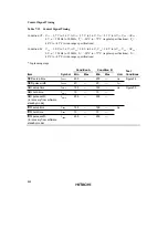
Timing of On-Chip Supporting Modules
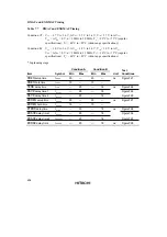
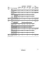
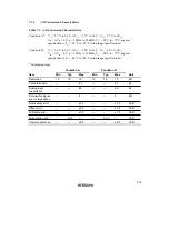
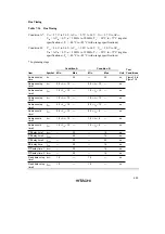
Table 7.8
Timing of On-Chip Supporting Modules
Condition A*: V
CC
= 2.7 V to 3.6 V, AV
CC
= 2.7 V to 3.6 V, V
ref
= 2.7 V to AV
CC
,
V
SS
= AV
SS
= 0 V, ø = 2 MHz to 20 MHz, T
a
= –20°C to +75°C (regular
specifications), T
a
= –40°C to +85°C (wide-range specifications)
Condition B:
V
CC
= 3.0 V to 3.6 V, AV
CC
= 3.0 V to 3.6 V, V
ref
= 3.0 V to AV
CC
,
V
SS
= AV
SS
= 0 V, ø = 2 MHz to 33 MHz, T
a
= –20°C to +75°C (regular
specifications), T
a
= –40°C to +85°C (wide-range specifications)
* In planning stage
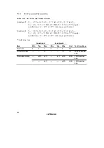
Condition A
Condition B
Test
Item
Symbol
Min
Max
Min
Max
Unit
Conditions
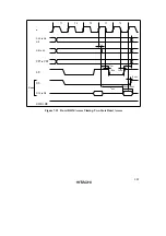
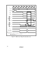
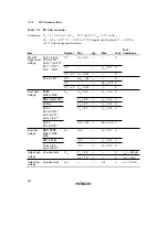
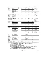
I/O ports
Output data delay
time
t
PWD
—
50
—
40
ns
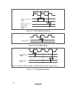
Figure7.29
Input data setup
time
t
PRS
30
—
25
—
ns
Input data hold time
t
PRH
30
—
25
—
ns
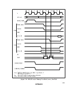
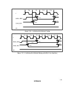
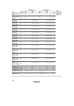
PPG
Pulse output delay
time
t
POD
—
50
—
40
ns
Figure7.30
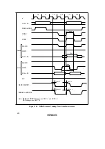
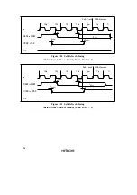
TPU
Timer output delay
time
t
TOCD
—
50
—
40
ns
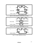
Figure7.31
Timer input setup
time
t
TICS
30
—
25
—
ns
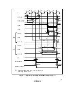
Timer clock input
setup time
t
TCKS
30
—
25
—
ns
Figure7.32
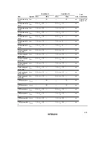
Timer
clock
Single-edge
specification
t
TCKWH
1.5
—
1.5
—
t
cyc
pulse
width
Both-edge
specification
t
TCKWL
2.5
—
2.5
—
t
cyc
Summary of Contents for H8S/2670
Page 5: ......
Page 9: ......
Page 199: ...182 ...
Page 361: ...344 ...
Page 393: ...376 ...
Page 647: ...630 ...


