525
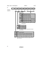
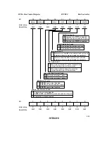
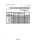
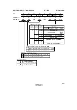
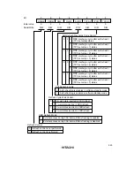
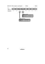
DRAMCR—DRAM Control Register
H'FED0
Bus Controller
Bit
Initial value
Read/Write
15
OEE
0
R/W
14
RAST
0
R/W
13
—
0
R/W
12
CAST
0
R/W
11
—
0
R/W
10
RMTS2
0
R/W
9
RMTS1
0
R/W
8
RMTS0
0
R/W
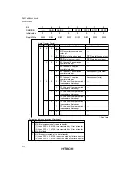
DRAM Space Select
RMTS0
Description
Area 5
Area 4
Area 3
Area 2
0
Normal space
Normal space
DRAM
space
Normal space
DRAM space
DRAM space
Reserved (setting prohibited)
Continuous DRAM space
RMTS1
0
RMTS2
0
1
0
1
1
—
0
1
0
1
1
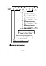
Column Address Output Cycle Number Select
0
Column address output cycle comprises 2 states
1
Column address output cycle comprises 3 states
RAS
Assertion Timing Select
0
RAS
is asserted from ø falling edge in T
r
cycle
1
RAS
is asserted from start of T
r
cycle
OE
Output Enable
0
OE
signal output disabled
OE
pin can be used as I/O port
1
OE
signal output enabled
Summary of Contents for H8S/2670
Page 5: ......
Page 9: ......
Page 199: ...182 ...
Page 361: ...344 ...
Page 393: ...376 ...
Page 647: ...630 ...

