201
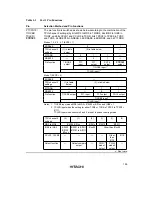
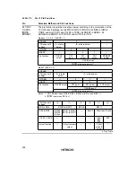
Pin
Selection Method and Pin Functions
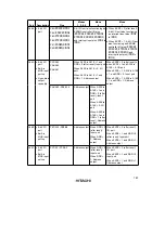
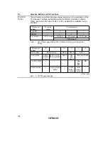
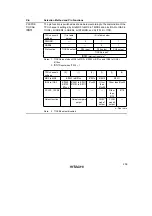
P11/PO9/
TIOCB0
The pin function is switched as shown below according to the combination of the
TPU channel 0 settings (by bits MD3 to MD0 in TMDR0 and bits IOB3 to IOB0 in
TIOR0H), bit NDER9 in NDERH, and bit P11DDR.
TPU channel 0
settings
(1) in table
below
(2) in table below
P11DDR
—
0
1
1
NDER9
—
—
0
1
Pin function
TIOCB0 output
P11 input
P11 output
PO9 output
TIOCB0 input
*
1
Note:
1. TIOCB0 input when MD3 to MD0 = B'0000 and IOB3 to IOB0 = B'10xx.
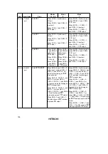
TPU channel 0
settings
(2)
(1)
(2)
(2)
(1)
(2)
MD3 to MD0
B'0000
B'0010
B'0011
IOB3 to IOB0
B'0000
B'0100
B'1xxx
B'0001 to B'0011
B'0101 to B'0111
—
B'xx00
Other than B'xx00
CCLR2, CCLR0
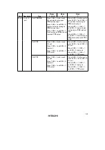
—
—
—
—
Other
than
B'010
B'010
Output function
—
Output compare
output
—
—
PWM
mode 2
output
—
x: Don’t care
Summary of Contents for H8S/2670
Page 5: ......
Page 9: ......
Page 199: ...182 ...
Page 361: ...344 ...
Page 393: ...376 ...
Page 647: ...630 ...

