457
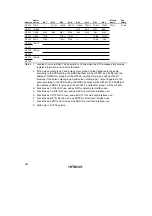
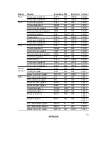
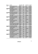
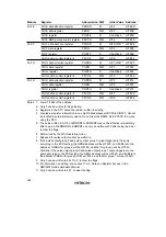
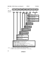
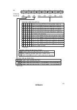
12. Flash memory registers are allocated to the same addresses as other registers.
Register selection is performed by means of the FLSHE bit in the system control
register (SYSCR).
13. In modes in which the on-chip flash memory is disabled, a read will return H'00, and
writes are invalid. Writes are also disabled when the FWE bit in FLMCR1 is cleared to
0.
14. When a high level is input to the FWE pin, the initial value is H'80.
15. When a low level is input to the FWE pin, or if a high level is input but the SWE bit in
FLMCR1 is not set, these registers are initialized to H'00.
16. FLMCR1, FLMCR2, EBR1, and EBR2 are 8-bit registers. Only byte access can be used
on these registers, with the access requiring two states.
17. The initial value depends on the mode.
18. Valid in the F-ZTAT version only.
Summary of Contents for H8S/2670
Page 5: ......
Page 9: ......
Page 199: ...182 ...
Page 361: ...344 ...
Page 393: ...376 ...
Page 647: ...630 ...

