108
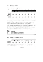
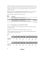
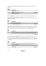
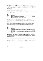
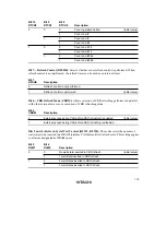
Bit 15
OEE
Description
0
OE
signal output disabled
OE
pin can be used as I/O port
(Initial value)
1
OE
signal output enabled
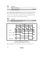
Bit 14—
RAS
Assertion Timing Select (RAST): Selects whether, in DRAM access, the
RAS
signal is asserted from the start of the T
r
cycle (rising edge of ø) or from the falling edge of ø.
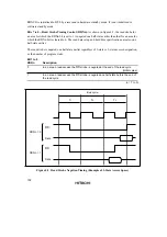
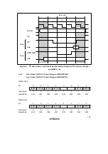
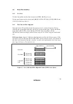
Figure 4.4 shows the relationship between the RAST bit setting and the
RAS
assertion timing.
The setting of this bit applies to all areas designated as DRAM space.
Bit 14
RAST
Description
0
RAS
is asserted from ø falling edge in T
r
cycle
(Initial value)
1
RAS
is asserted from start of T
r
cycle
T
p
Address
RAST = 0
RAS
RAST = 1
RAS
T
r
T
c1
T
c2
UCAS
,
LCAS
Bus cycle
Row address
Column address
Figure 4.4
RAS
Signal Assertion Timing
(2-State Column Address Output Cycle, Full Access)
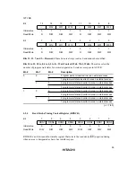
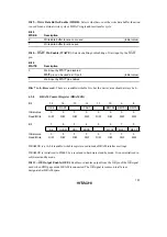
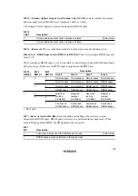
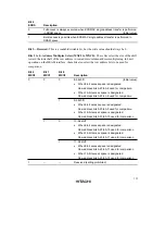
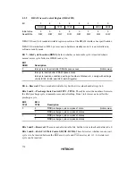
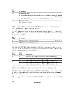
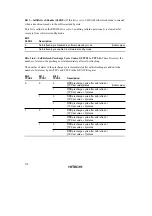
Bit 13—Reserved: This is a readable/writable bit, but the write value should always be 0.
Summary of Contents for H8S/2670
Page 5: ......
Page 9: ......
Page 199: ...182 ...
Page 361: ...344 ...
Page 393: ...376 ...
Page 647: ...630 ...

