143
4.5.8
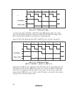
Row Address Output Cycle Control
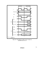
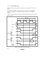
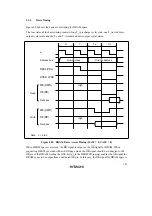
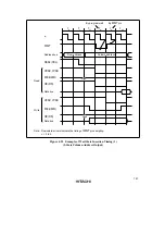
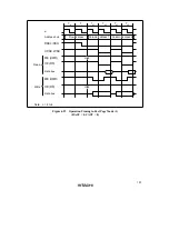
If the RAST bit is set to 1 in the DRAMCR register, the
RAS
signal goes low from the beginning
of the T
r
state, and the row address hold time and DRAM read access time are changed relative to
the fall of the
RAS
signal. Use the optimum setting according to the DRAM connected and the
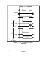
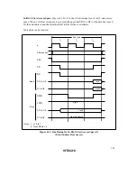
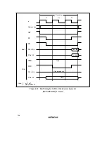
operating frequency of the chip. Figure 4.22 shows an example of the timing when the
RAS
signal
goes low from the beginning of the T
r
state.
T
p
ø
RASn
(
CSn
)
Read
Write
UCAS
,
LCAS
WE
(
HWR
)
OE
(
RD
)
Data bus
WE
(
HWR
)
OE
(
RD
)
Data bus
Address bus
T
r
T
c1
T
c2
Row address
Column address
High
High
Note: n = 2 to 5
Figure 4.22 Example of Access Timing when
RAS
Signal Goes Low from Beginning
of T
r
State (CAST = 0)
Summary of Contents for H8S/2670
Page 5: ......
Page 9: ......
Page 199: ...182 ...
Page 361: ...344 ...
Page 393: ...376 ...
Page 647: ...630 ...

