121
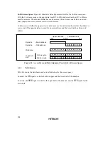
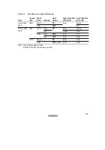
An area for which the basic bus interface is designated functions as normal space, an area for
which the DRAM interface is designated functions as DRAM space, and an area for which the
burst ROM interface is designated functions as burst ROM space.
The initial state of each area is basic bus interface, 3-state access space. The initial bus width is
selected according to the operating mode. The bus specifications described here cover basic items
only, and the sections on each memory interface (4.4, 4.5, and 4.6) should be referred to for
further details.
Area 0: Area 0 includes on-chip ROM*, and in expanded mode with on-chip ROM disabled, all of
area 0 is external space. In expanded mode with on-chip ROM enabled, the space excluding on-
chip ROM* is external space.
When area 0 external space is accessed, the
CS0
signal can be output.
Either basic bus interface or burst ROM interface can be selected for area 0.
Note:
* Applies only to versions with ROM.
Area 1: In externally expanded mode, all of area 1 is external space.
When area 1 external space is accessed, the
CS1
signal can be output.
Either basic bus interface or burst ROM interface can be selected for area 1.
Areas 2 to 5: In externally expanded mode, areas 2 to 5 are all external space.
When area 2 to 5 external space is accessed, signals
CS2
to
CS5
can be output.
Basic bus interface or DRAM interface can be selected for areas 2 to 5. With the DRAM interface,
signals
CS2
to
CS5
are used as
RAS
signals.
If areas 2 to 5 are designated as continuous DRAM space, large-capacity (e.g. 64-Mbit) DRAM
can be connected. In this case, the
CS2
signal is used as the
RAS
signal for the continuous DRAM
space.
Area 6: In externally expanded mode, all of area 6 is external space.
When area 6 external space is accessed, the
CS6
signal can be output.
Only the basic bus interface can be used for area 6.
Area 7: Area 7 includes the on-chip RAM and internal/O registers. In externally expanded mode,
the space excluding the on-chip RAM and internal I/O registers is external space. The on-chip
RAM is enabled when the RAME bit is set to 1 in the system control register (SYSCR); when the
RAME bit is cleared to 0, the on-chip RAM is disabled and the corresponding addresses are in
external space.
Summary of Contents for H8S/2670
Page 5: ......
Page 9: ......
Page 199: ...182 ...
Page 361: ...344 ...
Page 393: ...376 ...
Page 647: ...630 ...

