89
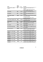
Interrupt Source
Origin of
Interrupt
Source
Vector
Number
Vector Address
Advanced Mode
DTCE
*
Priority
TGI3A (TGR3A compare
match/input capture)
TPU
channel 3
56
H'0470
DTCED5
High
TGI3B (TGR3B compare
match/input capture)
57
H'0472
DTCED4
TGI3C (TGR3C compare
match/input capture)
58
H'0474
DTCED3
TGI3D (TGR3D compare
match/input capture)
59
H'0476
DTCED2
TGI4A (TGR4A compare
match/input capture)
TPU
channel 4
64
H'0480
DTCED1
TGI4B (TGR4B compare
match/input capture)
65
H'0482
DTCED0
TGI5A (TGR5A compare
match/input capture)
TPU
channel 5
68
H'0488
DTCEE7
TGI5B (TGR5B compare
match/input capture)
69
H'048A
DTCEE6
CMI0A (compare match A)
8-bit timer
channel 0
72
H'0490
DTCEE3
CMI0B (compare match B)
73
H'0492
DTCEE2
CMI1A (compare match A)
8-bit timer
channel 1
76
H'0498
DTCEE1
CMI1B (compare match B)
77
H'049A
DTCEE0
DMTEND0A (channel 0/channel
0A transfer end)
DMAC
80
H'04A0
DTCEF7
DMTEND0B (channel 0B transfer
end)
81
H'04A2
DTCEF6
DMTEND1A (channel 1/channel
1A transfer end)
82
H'04A4
DTCEF5
DMTEND1B (channel 1B transfer
end)
83
H'04A6
DTCEF4
RXI0 (receive completed 0)
SCI channel 0
89
H'04B2
DTCEF3
TXI0 (transmit data empty 0)
90
H'04B4
DTCEF2
RXI1 (receive completed 1)
SCI channel 1
93
H'04BA
DTCEF1
TXI1 (transmit data empty 1)
94
H'04BC
DTCEF0
RXI2 (receive completed 2)
SCI channel 2
97
H'04C2
DTCEG7
TXI2 (transmit data empty 2)
98
H'04C4
DTCEG6
Low
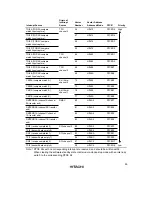
Note:
*
DTCE bits with no corresponding interrupt are reserved, and should be written with 0.
When clearing the software standby state or all-module-clocks-stop mode with an interrupt,
write 0 to the corresponding DTCE bit.
Summary of Contents for H8S/2670
Page 5: ......
Page 9: ......
Page 199: ...182 ...
Page 361: ...344 ...
Page 393: ...376 ...
Page 647: ...630 ...


