612
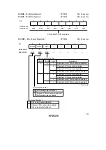
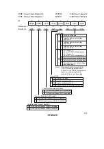
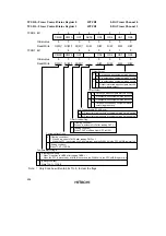
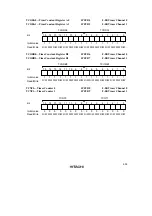
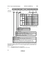
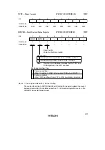
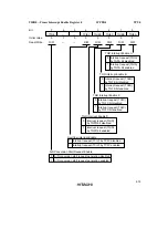
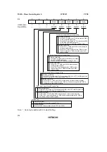
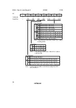
TMDR0—Timer Mode Register 0
H'FFD1
TPU0
Bit
Initial value
Read/Write
7
—
1
—
6
—
1
—
5
BFB
0
R/W
4
BFA
0
R/W
3
MD3
0
R/W
2
MD2
0
R/W
1
MD1
0
R/W
0
MD0
0
R/W
0
0
Normal operation
Reserved
PWM mode 1
PWM mode 2
Phase counting mode 1
Phase counting mode 2
Phase counting mode 3
Phase counting mode 4
Mode
1
1
*
0
1
0
1
*
0
1
0
1
0
1
0
1
*
*
: Don’t care
—
Notes: 1. MD3 is a reserved bit.
In a write, it should always be
written with 0.
2. Phase counting mode cannot
be set for channels 0 and 3.
In this case, 0 should always
be written to MD2.
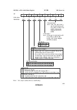
0 TGRA operates normally
TGRA and TGRC used together for buffer
operation
TGRA Buffer Operation
1
0 TGRB operates normally
TGRB and TGRD used together for buffer
operation
TGRB Buffer Operation
1
Summary of Contents for H8S/2670
Page 5: ......
Page 9: ......
Page 199: ...182 ...
Page 361: ...344 ...
Page 393: ...376 ...
Page 647: ...630 ...

