94
4.1.3
Pin Configuration
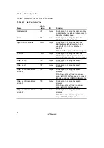
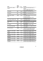
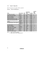
Table 4.1 summarizes the pins of the bus controller.
Table 4.1
Bus Controller Pins
Name
Abbre-
viation
I/O
Function
Address strobe
AS
Output
Strobe signal indicating that address output
on address bus is enabled during access to
basic bus interface space.
Read
RD
Output
Strobe signal indicating that basic bus
interface space is being read.
High write/write enable
HWR
Output
Strobe signal indicating that basic bus
interface space is being written to, and
upper half (D15 to D8) of data bus is
enabled.
DRAM interface space write enable signal.
Low write
LWR
Output
Strobe signal indicating that basic bus
interface space is being written to, and
lower half (D7 to D0) of data bus is enabled.
Chip select 0
CS0
Output
Strobe signal indicating that area 0 is
selected.
Chip select 1
CS1
Output
Strobe signal indicating that area 1 is
selected.
Chip select 2/row address
strobe 2
CS2
Output
Strobe signal indicating that area 2 is
selected.
DRAM row address strobe signal when
area 2 is DRAM interface space or areas 2
to 5 are continuous DRAM interface space.
Chip select 3/row address
strobe 3
CS3
Output
Strobe signal indicating that area 3 is
selected.
DRAM row address strobe signal when
area 3 is DRAM interface space.
Chip select 4/row address
strobe 4
CS4
Output
Strobe signal indicating that area 4 is
selected.
DRAM row address strobe signal when
area 4 is DRAM interface space.
Summary of Contents for H8S/2670
Page 5: ......
Page 9: ......
Page 199: ...182 ...
Page 361: ...344 ...
Page 393: ...376 ...
Page 647: ...630 ...

