218
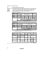
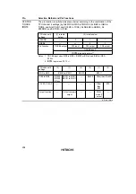
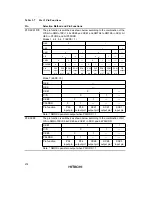
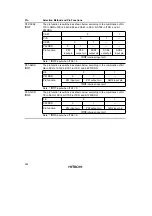
Table 5.7
Port 3 Pin Functions
Pin
Selection Method and Pin Functions
P35/SCK1/
OE
The pin function is switched as shown below according to the combination of the
C/
A
bit in SMR of SCI1, bits CKE0 and CKE1 and RMTS2 to RMTS0 in SCR, bit
OES in PFCR2, and bit P35DDR.
Modes 1, 2, 4, 5, 6, 7 (EXPE = 1)
OEE
0
1
OES
—
1
0
CKE1
0
1
0
1
—
C/
A
0
1
—
0
1
—
—
CKE0
0
1
—
—
0
1
—
—
—
P35DDR
0
1
—
—
—
0
1
—
—
—
—
Pin
function
P35
input
pin
P35
output
pin
*
SCK1
output
pin
*
SCK1
output
pin
*
SCK1
input
pin
P35
input
pin
P35
output
pin
*
SCK1
output
pin
*
SCK1
output
pin
*
SCK1
input
pin
OE
output
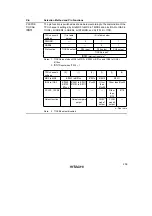
Mode 7 (EXPE = 0)
OEE
—
OES
—
CKE1
0
—
C/
A
0
1
—
CKE0
0
1
—
—
P35DDR
0
1
—
—
—
Pin function
P35
input pin
P35
output pin
*
SCK1
output pin
*
SCK1
output pin
*
SCK1
input pin
Note:
*
NMOS open-drain output when P35ODR = 1.
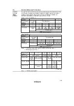
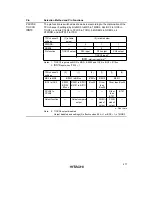
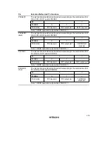
P34/SCK0
The pin function is switched as shown below according to the combination of bit
C/
A
in SMR of SCI0, bits CKE0 and CKE1 in SCR, and bit P34DDR.
CKE1
0
1
C/
A
0
1
—
CKE0
0
1
—
—
P34DDR
0
1
—
—
—
Pin function
P34
input pin
P34
output pin
*
SCK0
output pin
*
SCK0
output pin
*
SCK0
input pin
Note:
*
NMOS open-drain output when P34ODR = 1.
Summary of Contents for H8S/2670
Page 5: ......
Page 9: ......
Page 199: ...182 ...
Page 361: ...344 ...
Page 393: ...376 ...
Page 647: ...630 ...

