22
Pin No.
Type
Symbol
FP-144
I/O
Name and Function
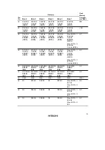
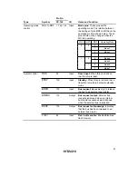
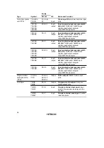
Interrupt signals
NMI
38
Input
Nonmaskable interrupt: Requests a
nonmaskable interrupt. Fix high when
not used.
IRQ15
to
IRQ0
(
IRQ15
) to
(
IRQ0
)
87, 86,
84 to 81,
61, 60,
130 to 127,
110 to 107,
59 to 52,
112, 111,
4 to 2,
142 to 140
Input
Interrupt request 15 to 0: These pins
request a maskable interrupt.
Address bus
A23 to A0
32 to 27,
25 to 20,
18 to 13,
11 to 6
Output
Address bus: These pins output an
address.
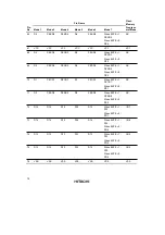
Data bus
D15 to D0
72 to 75,
77 to 80,
63 to 66,
68 to 71
Input/
output
Data bus: These pins constitute a
bidirectional data bus.
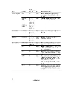
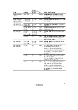
Bus control
CS7
to
CS0
112, 111,
106 to 101
Output
Chip select: Signals that select areas 7
to 0.
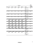
AS
91
Output
Address strobe: When this pin is low, it
indicates that address output on the
address bus is valid.
RD
90
Output
Read: When this pin is low, it indicates
that the external address space is being
read.
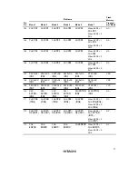
HWR
89
Output
High write/write enable: Strobe signal
indicating that external space is to be
written, and the upper half (D15 to D8)
of the data bus is enabled.
Write enable signal for DRAM interface
space.
LWR
88
Output
Low write: Strobe signal indicating that
external space is to be written, and the
lower half (D7 to D0) of the data bus is
enabled.
Summary of Contents for H8S/2670
Page 5: ......
Page 9: ......
Page 199: ...182 ...
Page 361: ...344 ...
Page 393: ...376 ...
Page 647: ...630 ...


