613
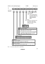
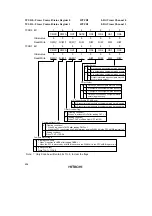
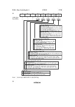
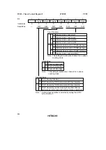
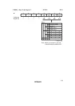
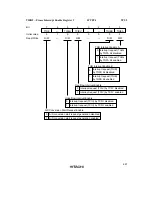
TIOR0H—Timer I/O Control Register 0H
H'FFD2
TPU0
Bit
Initial value
Read/Write
7
IOB3
0
R/W
6
IOB2
0
R/W
5
IOB1
0
R/W
4
IOB0
0
R/W
3
IOA3
0
R/W
2
IOA2
0
R/W
1
IOA1
0
R/W
0
IOA0
0
R/W
0
0
TGR0A I/O Control
0
0
1
TGR0A
is output
compare
register
1
0
1
1
0
0
1
1
0
1
0
1
0
0
TGR0A
is input
capture
register
1
1
*
Output disabled
Initial output is
1 output
Output disabled
Initial output is
0 output
Capture input
source is
TIOCA0 pin
0 output at compare match
1 output at compare match
Toggle output at compare match
*
: Don’t care
0 output at compare match
1 output at compare match
Toggle output at compare match
Input capture at rising edge
Input capture at falling edge
Input capture at both edges
*
*
1
Capture input
source is channel
1/count clock
Input capture at TCNT1 count-up/
count-down
0
0
TGR0B I/O Control
0
0
1
TGR0B
is output
compare
register
1
0
1
1
0
0
1
1
0
1
0
1
0
0
TGR0B
is input
capture
register
1
1
*
Output disabled
Initial output is
1 output
Output disabled
Initial output is
0 output
Capture input
source is
TIOCB0 pin
0 output at compare match
1 output at compare match
Toggle output at compare match
*
: Don’t care
0 output at compare match
1 output at compare match
Toggle output at compare match
Input capture at rising edge
Input capture at falling edge
Input capture at both edges
*
*
1
Capture input
source is channel
1/count clock
Input capture at TCNT1 count-up/
count-down
*
1
Note: 1. When bits TPSC2 to TPSC0 in TCR1 are set to B’000 and ø/1 is used as
the TCNT1 count clock, this setting is invalid and input capture does not
occur.
Summary of Contents for H8S/2670
Page 5: ......
Page 9: ......
Page 199: ...182 ...
Page 361: ...344 ...
Page 393: ...376 ...
Page 647: ...630 ...

