18. MR-J4W2-0303B6 SERVO AMPLIFIER
18 - 27
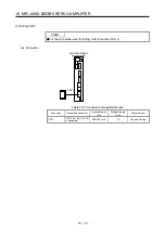
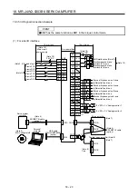
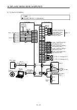
18.3.7 Signal (device) explanations
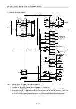
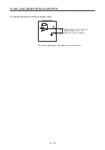
For the I/O interfaces (symbols in I/O division column in the table), refer to section 3.8.2 and section 18.3.9
(2).
The pin numbers in the connector pin No. column are those in the initial status.
(1) Input device
Device Symbol
Connector
pin No.
Function and application
I/O
division
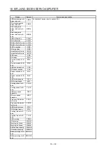
Forced stop 2
EM2
CN3-10
For details of device, refer to section 3.5.1.
DI-1
Forced stop 1
EM1
(CN3-10)
DI-1
DI1-A CN3-7
DI-1
DI2-A CN3-8
DI-1
DI3-A CN3-9
DI-1
DI1-B CN3-20
DI-1
DI2-B CN3-21
DI-1
DI3-B CN3-22
DI-1
(2) Output device
(a) Output device pin
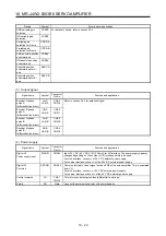
The following shows the output device pins and parameters for assigning devices.
Connector pin No.
Parameter
Initial device
I/O division
Remark
A-axis B-axis
CN3-12
[Pr. PD07]
MBR-A
For A-axis
CN3-25 [Pr.
PD07]
MBR-B
DO-1
For B-axis
CN3-11
[Pr. PD09]
[Pr. PD09]
CALM
Common pin
CN3-24
[Pr. PD08]
[Pr. PD08]
CINP
Common pin
(b) Output device explanations
POINT
Initial letter and last letter with hyphen in device symbols mean target axis. Refer
to the following table.
Symbol
(Note)
Target axis
Description
C _ _ _
A axis/B axis
When both axes of A and B meet a condition, the device will
be enabled (on or off).
X _ _ _
A axis/B axis
When each axis of A or B meets a condition, the device will
be enabled (on or off).
_ _ _ -A
A axis
Device for A axis
_ _ _ -B
B axis
Device for B axis
Note.
_ _ _ differs depending on devices.
Summary of Contents for MR-J4W2-0303B6
Page 39: ...2 INSTALLATION 2 8 MEMO ...
Page 97: ...4 STARTUP 4 20 MEMO ...
Page 181: ...6 NORMAL GAIN ADJUSTMENT 6 28 MEMO ...
Page 235: ...9 DIMENSIONS 9 6 MEMO ...
Page 245: ...10 CHARACTERISTICS 10 10 MEMO ...
Page 309: ...13 USING STO FUNCTION 13 14 MEMO ...
Page 365: ...15 USING A DIRECT DRIVE MOTOR 15 24 MEMO ...
Page 389: ...16 FULLY CLOSED LOOP SYSTEM 16 24 MEMO ...
Page 461: ...17 APPLICATION OF FUNCTIONS 17 72 MEMO ...
Page 556: ...APPENDIX App 41 ...
Page 585: ...MEMO ...

