INT8
INT3
INT2
ADC Sample
Generation
Logic
E
O
C
INT1
0
1
15
2
ADCINT1 to PIE
Latch
Set
Clear
INTSEL1N2.INT1SEL
EOC15:EOC0
INTSEL1N2.INT1E
1
0
1
0
INTSEL1N2.INT1CONT
ADCINTFLGCLR.ADCINT1
ADCINTFLG.ADCINT1
INTOVF
Analog-to-Digital Converter (ADC)
869
SPRUH22I – April 2012 – Revised November 2019
Copyright © 2012–2019, Texas Instruments Incorporated
Analog Subsystem
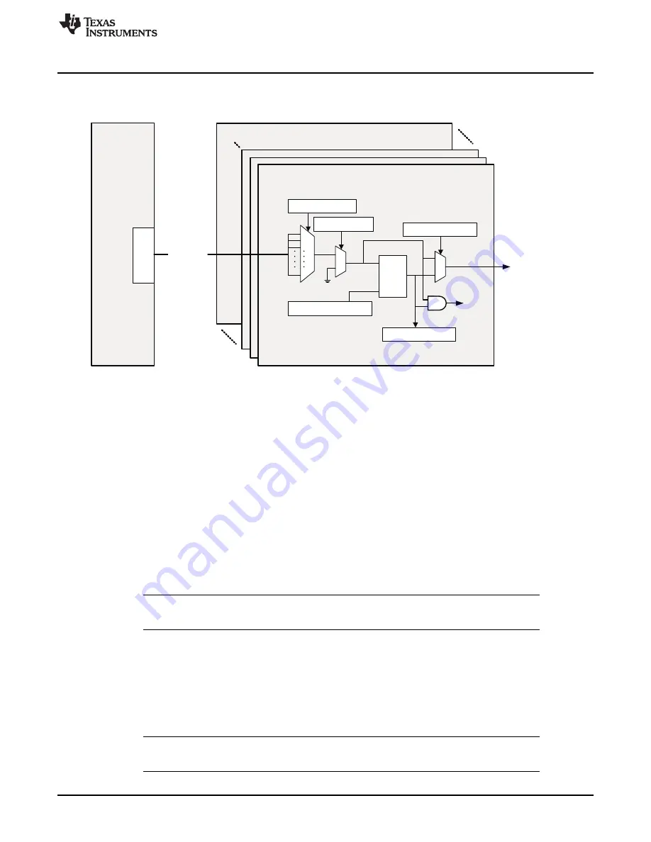
shows a block diagram of the interrupt structure of the ADC.
Figure 10-16. Interrupt Structure
10.3.8 Power Up Sequence
The ADC resets to the ADC off state. Before writing to any of the ADC registers the Analog Subsystem
clocks must be enabled. For a description on how to enable these clocks, see
. When
powering up the ADC, use the following sequence:
1. If an external reference is desired, enable this mode using bit 3 (ADCREFSEL) in the ADCCTL1
register.
2. Power up the reference, bandgap, and analog circuits together by setting bits 7-5 (ADCPWDN,
ADCBGPWD, ADCREFPWD) in the ADCCTL1 register. Intermediary states are not currently
supported.
3. Enable the ADC by setting bit 14 (ADCENABLE) of the ADCCTL1 register.
4. Before performing the first conversion, a delay of 1 millisecond after step 2 is required.
Alternatively, steps 1 through 3 can be performed simultaneously.
When powering down the ADC, all three bits in step 2 can be cleared simultaneously. The ADC power
levels must be controlled via software and they are independent of the state of the device power modes.
NOTE:
This type ADC requires a 1ms delay after all of the circuits are powered up. This differs from
the previous type ADC's.
10.3.9 ADC Calibration
Inherent in any converter is a zero offset error and a full scale gain error. The ADC is factory calibrated at
25-degrees Celsius to correct both of these while allowing the user to modify the offset correction for any
application environmental effects, such as the ambient temperature. Except under certain emulation
conditions, or unless a modification from the factory settings is desired, the user is not required to perform
any specific action. The ADC will be properly calibrated during the device boot process.
NOTE:
If the system is reset or the ADC module is reset using Bit 15 (RESET) from the ADC
Control Register 1, the Device_cal() routine must be repeated.


