


6-31
TI71M01D06-01EN 3rd Edition: 2012.12.01
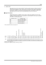
RY1
ON
OFF
MC
MC
MC
MC
RY1
LINE
CONT
LINE
MAIN
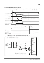
<TB1>
<TB4>
ERR+
ERR‑
※
L
L
N
N
5
6
*2
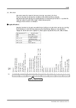
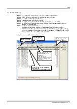
Line filter
Circuit
protector
Power
supply
Note
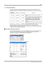
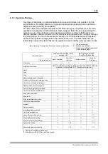
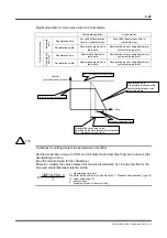
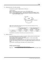
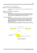
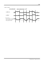
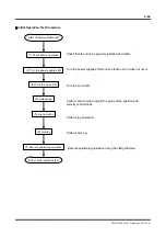
6.1.7 Signal Timing when Turning the Power ON
Make sure that the signals observe the sequence shown in the following timing diagram when
the power is turned ON.
*1 Waveform when the logic setting is positive and no error occurs when the power is turned ON
*2 The timing diagram shows the timing for the circuit configuration shown in the figure below.
Note: Main power supply on switch
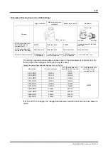
Example of power supply sequence circuit
Main power supply input *2
Control power supply input
Main power supply status
Regeneration error output
(TB4)
Main power supply on switch
(external circuit)
Rush interval
Constant supply status
External circuit delay
1sec or less
4sec or less
50msec or more
IN_
(CN4 I/O input)
I/O input signals are ignored during this period.
OUT_DRDY*1
(CN4 drive (CPU) ready)
I/O operation start
1.2sec
0.5sec
Drive