FFULL
(
)
EPI0S27
FEMPTY
(
)
EPI0S26
CS
(
)
EPI0S30
WR
(
)
EPI0S29
RD
(
)
EPI0S28
Data
Data
Data
Addr2
OE
Address
Data
Addr1
Addr3
Data2
Data1
Data3
Data
ALE
(
)
EPI0S30
CS0/CS1/CS2/CS3
(
/
EPI0S26 EPI0S27/
EPI0S34 EPI0S33)
/
WR
(
)
EPI0S29
RD/OE
(
)
EPI0S28
Address
(high order, non-muxed)
Muxed
Address/Data
Address
BSEL0/ BSEL1
a
a
BSEL0 and BSEL1 are available in Host-Bus16 mode only.
Host Bus Mode
1251
SPRUHE8E – October 2012 – Revised November 2019
Copyright © 2012–2019, Texas Instruments Incorporated
External Peripheral Interface (EPI)
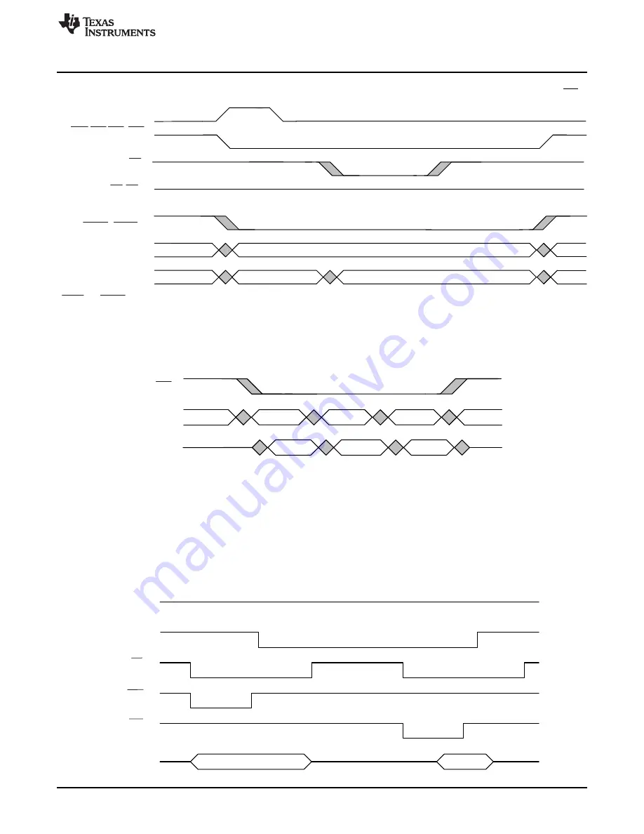
Figure 17-11. Host-Bus Write Cycle with Multiplexed Address and Data and ALE with Dual or Quad CS
shows continuous read mode accesses. In this mode, reads are performed by keeping the
read mode selected (output enable is asserted) and then changing the address pins. The data pins are
changed by the SRAM after the address pins change.
Figure 17-12. Continuous Read Mode Accesses
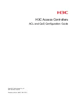
FIFO mode accesses are the same as normal read and write accesses, except that the ALE signal and
address pins are not present. Two input signals can be used to indicate when the XFIFO is full or empty to
gate transactions and avoid overruns and underruns. The FFULL and FEMPTY signals are synchronized
and must be recognized as asserted by the microcontroller for two system clocks before they affect
transaction status. The MAXWAIT field in the EPIHBnCFG register defines the maximum number of EPI
clocks to wait while the FEMPTY or FFULL signal is holding off a transaction.
shows how the
FEMPTY signal should respond to a write and read from the XFIFO.
shows how the
FEMPTY and FFULL signals should respond to two writes and one read from an external FIFO that
contains two entries.
Figure 17-13. Write Followed by Read to External FIFO


