Section 17 Synchronous Serial Communication Unit (SSU)
Rev. 1.00 Mar. 12, 2008 Page 565 of 1178
REJ09B0403-0100
17.4.3
Relationship between Data Input/Output Pins and Shift Register
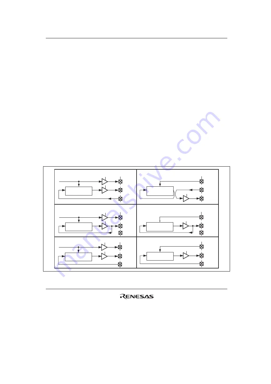
The connection between data input/output pins and the SS shift register (SSTRSR) depends on the
combination of the MSS and BIDE bits in SSCRH and the SSUMS bit in SSCRL. Figure 17.3
shows the relationship.
The SSU transmits serial data from the SSO pin and receives serial data from the SSI pin when
operating with BIDE
=
0 and MSS
=
1 (standard, master mode) (see figure 17.3 (1)). The SSU
transmits serial data from the SSI pin and receives serial data from the SSO pin when operating
with BIDE
=
0 and MSS
=
0 (standard, slave mode) (see figure 17.3 (2)).
The SSU transmits and receives serial data from the SSO pin regardless of master or slave mode
when operating with BIDE
=
1 (bidirectional mode) (see figures 17.3 (3) and (4)).
However, even if both the TE and RE bits are set to 1, transmission and reception are not
performed simultaneously. Either the TE or RE bit must be selected.
The SSU transmits serial data from the SSO pin and receives serial data from the SSI pin when
operating with SSUMS
=
1. The SSCK pin outputs the internal clock when MSS = 1 and function
as an input pin when MSS = 0 (see figures 17.3 (5) and (6)).
SSCK
Shift register
(SSTRSR)
Shift register
(SSTRSR)
Shift register
(SSTRSR)
Shift register
(SSTRSR)
SSO
SSI
SSCK
SSO
SSI
SSCK
SSO
SSI
SSCK
SSO
SSI
(1) When SSUMS = 0, BIDE = 0 (standard mode),
MSS = 1, TE = 1, and RE = 1
SSCK
Shift register
(SSTRSR)
SSO
SSI
SSCK
Shift register
(SSTRSR)
SSO
SSI
(2) When SSUMS = 0, BIDE = 0 (standard mode),
MSS = 0, TE = 1, and RE = 1
(3) When SSUMS = 0, BIDE = 1 (bidirectional mode),
MSS = 0, and either TE or RE = 1
(4) When SSUMS = 0, BIDE = 1 (bidirectional mode),
MSS = 1, and either TE or RE = 1
(5) When SSUMS = 1 and MSS = 1
(6) When SSUMS = 1 and MSS = 0
Figure 17.3 Relationship between Data Input/Output Pins and the Shift Register
Summary of Contents for H8S Family
Page 2: ...Rev 1 00 Mar 12 2008 Page ii of xIviii...
Page 8: ...Rev 1 00 Mar 12 2008 Page viii of xIviii...
Page 28: ...Rev 1 00 Mar 12 2008 Page xxviii of xIviii...
Page 48: ...Rev 1 00 Mar 12 2008 Page xlviii of xIviii...
Page 70: ...Section 1 Overview Rev 1 00 Mar 12 2008 Page 22 of 1178 REJ09B0403 0100...
Page 108: ...Section 2 CPU Rev 1 00 Mar 12 2008 Page 60 of 1178 REJ09B0403 0100...
Page 116: ...Section 3 MCU Operating Modes Rev 1 00 Mar 12 2008 Page 68 of 1178 REJ09B0403 0100...
Page 152: ...Section 5 Interrupt Controller Rev 1 00 Mar 12 2008 Page 104 of 1178 REJ09B0403 0100...
Page 206: ...Section 6 Bus Controller BSC Rev 1 00 Mar 12 2008 Page 158 of 1178 REJ09B0403 0100...
Page 420: ...Section 9 14 Bit PWM Timer PWMX Rev 1 00 Mar 12 2008 Page 372 of 1178 REJ09B0403 0100...
Page 476: ...Section 12 Watchdog Timer WDT Rev 1 00 Mar 12 2008 Page 428 of 1178 REJ09B0403 0100...
Page 552: ...Section 14 CRC Operation Circuit CRC Rev 1 00 Mar 12 2008 Page 504 of 1178 REJ09B0403 0100...
Page 712: ...Section 18 I2 C Bus Interface IIC Rev 1 00 Mar 12 2008 Page 664 of 1178 REJ09B0403 0100...
Page 804: ...Section 19 LPC Interface LPC Rev 1 00 Mar 12 2008 Page 756 of 1178 REJ09B0403 0100...
Page 838: ...Section 20 Ethernet Controller EtherC Rev 1 00 Mar 12 2008 Page 790 of 1178 REJ09B0403 0100...
Page 964: ...Section 24 RAM Rev 1 00 Mar 12 2008 Page 916 of 1178 REJ09B0403 0100...
Page 1066: ...Section 25 Flash Memory Rev 1 00 Mar 12 2008 Page 1018 of 1178 REJ09B0403 0100...
Page 1098: ...Section 26 Boundary Scan JTAG Rev 1 00 Mar 12 2008 Page 1050 of 1178 REJ09B0403 0100...
Page 1226: ...Rev 1 00 Mar 12 2008 Page 1178 of 1178 REJ09B0403 0100...
Page 1229: ......
Page 1230: ...H8S 2472 Group H8S 2462 Group Hardware Manual...


