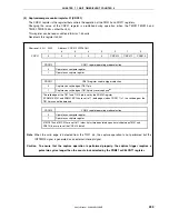
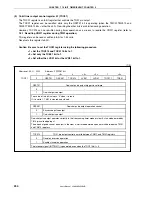
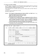
background image

CHAPTER  7   16-BIT  TIMER/EVENT  COUNTER  0 

User’s Manual  U16896EJ2V0UD 

236 

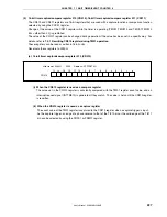
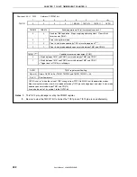
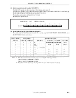
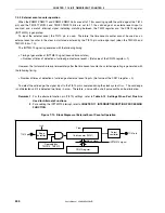
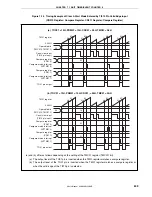
(4)  Prescaler mode register 01 (PRM01) 

The PRM01 register is the register that sets the TM01 register count clock and TI010 and TI011 pin input valid 

edges.  The PRM011 and PRM010 bits are set in combination with the SELCNT1.ISEL11 bit.  Refer to 

7.3 (6)  

Count clock setting for 16-bit timer/event counter 01

 for details. 

Rewriting the PRM01 register is prohibited during operation (when the TMC01.TMC013 and TMC01.TMC012 bits 

= other than 00). 

This register can be read or written in 8-bit or 1-bit units.   

Reset sets this register to 00H. 


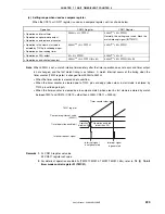
Cautions  1.  Do not apply the following setting when setting the PRM011 and PRM010 bits to 11 (to 

specify the valid edge of the TI010 pin as a count clock). 


  Clear & start mode entered by the TI010 pin valid edge  


  Setting the TI010 pin as a capture trigger 


2.  If the operation of the 16-bit timer/event counter 01 is enabled when the TI010 or TI011 pin is 

at high level and when the valid edge of the TI010 or TI011 pin is specified to be the rising 

edge or both edges, the high level of the TI010 or TI011 pin is detected as a rising edge.  

Note this when the TI010 or TI011 pin is pulled up.  However, the rising edge is not detected 

when the timer operation has been once stopped and is then enabled again. 

3.  When the P35 pin is used as the valid edge of TI010 and the timer output function is used, 

set the P32 pin as the timer output pin (TO01). 


ES111 

ES110 

TI011 pin valid edge selection 

0 0 

Falling 

edge 

0 1 

Rising 

edge 

1 0 

Setting 

prohibited 

Both falling and rising edges 


ES101 

ES100 

TI010 pin valid edge selection 

0 0 

Falling 

edge 

0 1 

Rising 

edge 

1 0 

Setting 

prohibited 

Both falling and rising edges 


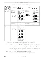
Remark

  For setting of the PRM011 and PRM010 bits, refer to 

7.3 (6)  Count clock setting for 16-bit 

timer/event counter 01


After reset:  00H     R/W 

Address:  

FFFFF617H  


7 6 5 4 3 2 1 0 

PRM01  ES111 ES110 ES101 ES100 

0  PRM011 

PRM010 

Summary of Contents for ?PD703302

Page 1: ...ES KE1 32 bit Single Chip Microcontrollers Hardware Printed in Japan User s Manual μPD703302 μPD703302Y μPD70F3302 μPD70F3302Y 2004 Document No U16896EJ2V0UD00 2nd edition Date Published August 2006 N CP K ...

Page 2: ...User s Manual U16896EJ2V0UD 2 MEMO ...

Page 3: ... including work benches and floors should be grounded The operator should be grounded using a wrist strap Semiconductor devices must not be touched with bare hands Similar precautions need to be taken for PW boards with mounted semiconductor devices STATUS BEFORE INITIALIZATION Power on does not necessarily define the initial status of a MOS device Immediately after the power source is turned ON d...

Page 4: ... United States of America EEPROM is a trademark of NEC Electronics Corporation Windows and Windows NT are either registered trademarks or trademarks of Microsoft Corporation in the United States and or other countries SuperFlash is a registered trademark of Silicon Storage Technology Inc in several countries including the United States and Japan PC AT is a trademark of International Business Machi...

Page 5: ...afety of NEC Electronics products customers agree and acknowledge that the possibility of defects thereof cannot be eliminated entirely To minimize risks of damage to property or injury including death to persons arising from defects in NEC Electronics products customers must incorporate sufficient safety measures in their design such as redundancy fire containment and anti failure features NEC El...

Page 6: ...s of electrical engineering logic circuits and microcontrollers To find the details of a register where the name is known Refer to APPENDIX C REGISTER INDEX To understand the details of an instruction function Refer to the V850ES Architecture User s Manual Register format The name of the bit whose number is in angle brackets in the figure of the register format of each register is defined as a res...

Page 7: ...ns However preliminary versions are not marked as such Documents related to V850ES KE1 Document Name Document No V850ES Architecture User s Manual U15943E V850ES KE1 Hardware User s Manual This manual Documents related to development tools user s manuals Document Name Document No QB V850MINI On Chip Debug Emulator U17638E QB V850ESKX1H In Circuit Emulator U17214E Operation U17293E C Language U1729...

Page 8: ...on of Unused Pins 36 2 3 Pin I O Circuits 38 CHAPTER 3 CPU FUNCTIONS 40 3 1 Features 40 3 2 CPU Register Set 41 3 2 1 Program register set 42 3 2 2 System register set 43 3 3 Operating Modes 49 3 4 Address Space 50 3 4 1 CPU address space 50 3 4 2 Wraparound of CPU address space 51 3 4 3 Memory map 52 3 4 4 Areas 54 3 4 5 Recommended use of address space 56 3 4 6 Peripheral I O registers 58 3 4 7 ...

Page 9: ...0 6 5 1 Interval timer mode TP0MD2 to TP0MD0 bits 000 151 6 5 2 External event count mode TP0MD2 to TP0MD0 bits 001 161 6 5 3 External trigger pulse output mode TP0MD2 to TP0MD0 bits 010 169 6 5 4 One shot pulse output mode TP0MD2 to TP0MD0 bits 011 181 6 5 5 PWM output mode TP0MD2 to TP0MD0 bits 100 188 6 5 6 Free running timer mode TP0MD2 to TP0MD0 bits 101 197 6 5 7 Pulse width measurement mode...

Page 10: ...5 8 4 5 Operation as interval timer 16 bits 308 8 4 6 Operation as external event counter 16 bits 310 8 4 7 Square wave output operation 16 bit resolution 311 8 4 8 Cautions 312 CHAPTER 9 8 BIT TIMER H 313 9 1 Functions 313 9 2 Configuration 313 9 3 Registers 316 9 4 Operation 320 9 4 1 Operation as interval timer square wave output 320 9 4 2 PWM output mode operation 323 9 4 3 Carrier generator m...

Page 11: ...4 Registers 368 13 5 Operation 377 13 5 1 Basic operation 377 13 5 2 Trigger modes 378 13 5 3 Operation modes 379 13 5 4 Power fail detection function 382 13 5 5 Setting method 383 13 6 Cautions 385 13 7 How to Read A D Converter Characteristics Table 391 CHAPTER 14 ASYNCHRONOUS SERIAL INTERFACE UART 395 14 1 Features 395 14 2 Configuration 396 14 3 Registers 398 14 4 Interrupt Request Signals 407...

Page 12: ...rol Methods 478 16 5 1 Start condition 478 16 5 2 Addresses 479 16 5 3 Transfer direction specification 479 16 5 4 ACK 480 16 5 5 Stop condition 481 16 5 6 Wait state 482 16 5 7 Wait state cancellation method 484 16 6 I2 C Interrupt Request Signals INTIIC0 485 16 6 1 Master device operation 486 16 6 2 Slave device operation when receiving slave address match with address 489 16 6 3 Slave device op...

Page 13: ...rrupts 543 17 3 4 Interrupt control register xxlCn 547 17 3 5 Interrupt mask registers 0 1 3 IMR0 IMR1 IMR3 549 17 3 6 In service priority register ISPR 550 17 3 7 ID flag 551 17 3 8 Watchdog timer mode register 1 WDTM1 552 17 4 External Interrupt Request Input Pins NMI INTP0 to INTP7 553 17 4 1 Noise elimination 553 17 4 2 Edge detection 555 17 5 Software Exceptions 559 17 5 1 Operation 559 17 5 ...

Page 14: ...heck Reset Source 590 20 4 Reset Sources 591 20 4 1 Reset operation via RESET pin 591 20 4 2 Reset operation by WDTRES1 signal 595 20 4 3 Reset operation by WDTRES2 signal 596 20 4 4 Power on clear reset operation 597 20 4 5 Reset operation by low voltage detector 600 20 4 6 Reset operation by clock monitor 601 20 5 Reset Output Function 602 CHAPTER 21 CLOCK MONITOR 603 21 1 Function 603 21 2 Regi...

Page 15: ...3 Functional Outline 628 26 4 Rewriting by Dedicated Flash Programmer 632 26 4 1 Programming environment 632 26 4 2 Communication mode 633 26 4 3 Flash memory control 638 26 4 4 Selection of communication mode 639 26 4 5 Communication commands 640 26 4 6 Pin connection 641 26 5 Rewriting by Self Programming 646 26 5 1 Overview 646 26 5 2 Features 647 26 5 3 Standard self programming flow 648 26 5 ...

Page 16: ...A 4 1 When using IECUBE QB V850ESKX1H 684 A 4 2 When using MINICUBE QB V850MINI 686 A 5 Debugging Tools Software 688 A 6 Embedded Software 689 A 7 Flash Memory Writing Tools 689 APPENDIX B INSTRUCTION SET LIST 690 B 1 Conventions 690 B 2 Instruction Set in Alphabetical Order 693 APPENDIX C REGISTER INDEX 700 APPENDIX D REVISION HISTORY 706 D 1 Major Revisions in This Edition 706 R R ...

Page 17: ...B RAM 12 KB V850ES KF1 PD70F3308Y PD70F3308 Single power flash 256 KB RAM 12 KB PD703308Y PD703308 Mask ROM 256 KB RAM 12 KB PD703214Y PD703214 Mask ROM 128 KB RAM 6 KB PD703213Y PD703213 Mask ROM 96 KB RAM 4 KB PD70F3214HY PD70F3214H Single power flash 128 KB RAM 6 KB PD70F3311Y PD70F3311 Single power flash 128 KB RAM 6 KB PD70F3214Y PD70F3214 Two power flash 128 KB RAM 6 KB PD703212Y PD703212 Ma...

Page 18: ...ch Automatic transmit receive 3 wire CSI 1 ch 2 ch 2 ch UART 1 ch 1 ch 2 ch 2 ch UART supporting LIN bus 1 ch 1 ch 1 ch 1 ch Serial interface I2 CNote 2 1 ch 1 ch 1 ch 2 ch Address space 128 KB 3 MB 15 MB Address bus 16 bits 22 bits 24 bits External bus Mode Multiplex only Multiplex separate DMA controller 4 ch 4 ch 10 bit A D converter 8 ch 8 ch 8 ch 16 ch 8 bit D A converter 2 ch 2 ch External 9...

Page 19: ...TO 6 bits 1 ch 6 bits 1 ch 6 bits 1 ch 6 bits 2 ch CSI 2 ch 2 ch 2 ch 3 ch Automatic transmit receive 3 wire CSI 1 ch 2 ch 2 ch UART 2 ch 2 ch 2 ch 3 ch UART supporting LIN bus Serial interface I2 CNote 2 1 ch 1 ch 1 ch 2 ch Address space 128 KB 3 MB 15 MB Address bus 16 bits 22 bits 24 bits External bus Mode Multiplex only Multiplex separate DMA controller 10 bit A D converter 8 ch 8 ch 8 ch 16 c...

Page 20: ... 1 KB Single power flash 24 KB RAM 1 KB Single power flash 16 KB RAM 512 B 78K0 KD1 PD78F0123H PD78F0124H HDNote PD78F0122H 78K0 KD1 Two power flash 32 KB RAM 1 KB PD78F0148 Mask ROM 60 KB RAM 2 KB PD780148 Mask ROM 48 KB RAM 2 KB PD780146 Mask ROM 32 KB RAM 1 KB PD780144 Mask ROM 24 KB RAM 1 KB PD780143 80 pin TQFP QFP 12 12 mm 0 5 mm pitch 14 14 mm 0 65 mm pitch Single power flash 60 KB RAM 2 KB...

Page 21: ...h For watch 1 ch Timer WDT 1 ch 3 wire CSI Note 3 1 ch 2 ch 1 ch 2 ch Automatic transmit receive 3 wire CSI 1 ch UART Note 3 1 ch Serial interface UART supporting LIN bus 1 ch 10 bit A D converter 4 ch 8 ch External 6 7 8 9 9 Interrupt Internal 11 12 15 16 19 17 20 Key return input 4 ch 8 ch RESET pin Provided POC 2 85 V 0 15 V 3 5 V 0 20 V selectable by mask option LVI 2 85 V 3 1 V 3 3 V 0 15 V 3...

Page 22: ...2 ch 8 bits TMH 2 ch For watch 1 ch Timer WDT 1 ch 3 wire CSI Note 2 1 ch 2 ch Automatic transmit receive 3 wire CSI 1 ch UART Note 2 1 ch Serial interface UART supporting LIN bus 1 ch 10 bit A D converter 4 ch 8 ch External 6 7 8 9 9 Interrupts Internal 11 12 15 16 19 20 Key return input 4 ch 8 ch RESET pin Provided POC 2 1 V 0 1 V detection voltage is fixed LVI 2 35 V 2 6 V 2 85 V 3 1 V 3 3 V 0 ...

Page 23: ... trap 1 source I O lines Total 51 Key interrupt function Timer function 16 bit timer event counter P 1 channel 16 bit timer event counter 0 1 channel 8 bit timer event counter 5 2 channels 8 bit timer H 2 channels 8 bit interval timer BRG 1 channel Watch timer interval timer 1 channel Watchdog timers Watchdog timer 1 also usable as oscillation stabilization timer 1 channel Watchdog timer 2 1 chann...

Page 24: ... reception etc Submicrocontroller of control system Home audio car audio AV equipment PC peripheral devices keyboards etc Household appliances Outdoor units of air conditioners Microwave ovens rice cookers Industrial devices Pumps Vending machines FA 1 4 Ordering Information Part Number Package Quality Grade μPD703302GK 9ET A μPD703302GB 8EU A μPD703302YGK 9ET A μPD703302YGB 8EU A μPD70F3302GK 9ET...

Page 25: ... TO01 P33 TIP00 TOP00 P34 TIP01 TOP01 P35 TI010 TO01 P50 KR0 TI011 RTP00 P51 KR1 TI50 RTP01 P52 KR2 TO50 RTP02 P53 KR3 RTP03 EV SS PDL1 PDL0 PCM1 CLKOUT PCM0 P915 INTP6 P914 INTP5 P913 INTP4 P99 SCK01 P98 SO01 P97 SI01 P96 TI51 TO51 P91 KR7 RXD1 P90 KR6 TXD1 P55 KR5 RTP05 P54 KR4 RTP04 EVDD AVREF0 AVSS ICNote 1 FLMD0Note 1 VDD NCNote 2 VSS X1 X2 RESET XT1 XT2 P00 TOH0 P01 TOH1 P02 NMI P03 INTP0 P0...

Page 26: ... connection NMI Non maskable interrupt request P00 to P06 Port 0 P30 to P35 P38 P39 Port 3 P40 to P42 Port 4 P50 to P55 Port 5 P70 to P77 Port 7 P90 P91 P96 to P99 P913 to P915 Port 9 PCM0 PCM1 Port CM PDL0 to PDL7 Port DL RESET Reset RTP00 to RTP05 Real time output port RXD0 RXD1 Receive data SCK00 SCK01 Serial clock SCL0 Serial clock SDA0 Serial data SI00 SI01 Serial input SO00 SO01 Serial outpu...

Page 27: ...o P06 AV REF0 AV SS ANI0 to ANI7 ADTRG ICNote 3 EVDD EVSS FLMD0 FLMD1Note 4 VSS BCU POC LVI CG CLKOUT X1 X2 XT1 XT2 RESET VDD 16 bit timer event counter 0 1 ch 16 bit timer event counter P 1 ch 8 bit timer event counter 5 2 ch 8 bit timer H 2 ch Note 1 4 KB ROM correction General purpose registers 32 bits 32 System registers 32 bit barrel shifter Multiplier 16 16 32 Instruction queue UART 2 ch I2 ...

Page 28: ...interrupt priorities can be specified for these interrupt requests and multiplexed servicing control can be performed f Clock generator CG A main clock oscillator and subclock oscillator are provided and generate the main clock oscillation frequency fX and subclock frequency fXT respectively There are two modes In the clock through mode fX is used as the main clock frequency fXX as is In the PLL m...

Page 29: ...I0n and SCK0n pins For I2 C0 data is transferred via the SDA0 and SCL0 pins I 2 C0 is provided only in the μPD703302Y and 70F3302Y Remark n 0 1 k A D converter This high speed high resolution 10 bit A D converter includes 8 analog input pins Conversion is performed using the successive approximation method l ROM correction This function is used to replace part of a program in the mask ROM with tha...

Page 30: ... below the following ports have general purpose port functions and control pin functions Port I O Alternate Function P0 7 bit I O NMI external interrupt timer output P3 8 bit I O Serial interface timer I O external interrupt A D converter trigger P4 3 bit I O Serial interface P5 6 bit I O Timer I O key interrupt function real time output function P7 8 bit input A D converter analog input P9 9 bit ...

Page 31: ...rain output selectable 4 fixed to N ch open drain output 2 Timer 16 bit timer event counter P 1 channel 16 bit timer event counter 0 1 channel 8 bit timer event counter 5 2 channels 16 bit timer event counter Usable as 1 channel 8 bit timer H 2 channels Watchdog timer 2 channels Watch timer 1 channel 8 bit interval timer 1 channel Real time output port 4 bits 1 2 bits 1 or 6 bits 1 A D converter 1...

Page 32: ...ction P00 12 TOH0 P01 13 TOH1 P02 14 NMI P03 15 INTP0 P04 16 INTP1 P05 17 INTP2 P06 18 I O Yes Port 0 I O port Input output can be specified in 1 bit units INTP3 P30 22 TXD0 P31 23 RXD0 INTP7 P32 24 ASCK0 ADTRG TO01 P33 25 TIP00 TOP00 P34 26 TIP01 TOP01 P35 27 Yes TI010 TO01 P38 55 SDA0 Note 2 P39 56 I O No Note 1 Port 3 I O port Input output can be specified in 1 bit units P38 and P39 are fixed t...

Page 33: ...58 ANI6 P77 57 Input No Port 7 Input port ANI7 P90 36 TXD1 KR6 P91 37 RXD1 KR7 P96 38 TI51 TO51 P97 39 SI01 P98 40 SO01 P99 41 SCK01 P913 42 INTP4 P914 43 INTP5 P915 44 I O Yes Port 9 I O port Input output can be specified in 1 bit units P98 and P99 can be specified as N ch open drain output in 1 bit units INTP6 PCM0 45 PCM1 46 I O Yes Port CM I O port Input output can be specified in 1 bit units ...

Page 34: ... 32 Ground potential for external FLMD0 Note 1 3 No FLMD1 Note 1 52 Input Yes Flash programming mode setting pin PDL5 IC Note 2 3 Internally connected INTP0 15 P03 INTP1 16 P04 INTP2 17 External interrupt request input maskable analog noise elimination P05 INTP3 18 External interrupt request input maskable digital analog noise elimination P06 INTP4 42 P913 INTP5 43 P914 INTP6 44 P915 INTP7 23 Inpu...

Page 35: ...n output can be specified in 1 bit units P98 TI010 27 Capture trigger input external event input for TM01 P35 TO01 TI011 28 Capture trigger input for TM01 P50 RTP00 KR0 TI50 29 External event input for TM50 P51 RTP01 KR1 TI51 38 External event input for TM51 P96 TO51 TIP00 25 Capture trigger input external event input for TMP0 P33 TOP00 TIP01 26 Input Yes Capture trigger input for TMP0 P34 TOP01 2...

Page 36: ... E P42 SCK00 21 10 F P50 TI011 RTP00 KR0 28 P51 TI50 RTP01 KR1 29 P52 TO50 RTP02 KR2 30 P53 RTP03 KR3 31 8 A P54 RTP04 KR4 34 P55 RTP05 KR5 35 10 A Input Independently connect to EVDD or EVSS via a resistor Output Leave open P70 to P77 ANI0 to ANI7 64 to 57 9 C Connect to AVREF0 or AVSS P90 TXD1 KR6 36 P91 RXD1 KR7 37 P96 TI51 TO51 38 8 A P97 SI01 39 5 W P98 SO01 40 10 E P99 SCK01 41 10 F P913 to ...

Page 37: ... to EVSS or VSS or pull down with a 10 kΩ resistor NC 5 Leave open RESET 9 2 Connect to EVDD via a resistor FLMD0 Note 2 3 Directly connect to EVSS or VSS or pull down with a 10 kΩ resistor VDD 4 VSS 6 X1 7 X2 8 XT1 10 16 Directly connect to VSS Note 3 XT2 11 16 Leave open Notes 1 Only in the μPD703302 703302Y 2 Only in the μPD70F3302 70F3302Y 3 Be sure to set the PSMR XTSTP bit to 1 when this pin...

Page 38: ...rator AVREF0 threshold voltage P ch N ch Input enable Pull up enable Data Output disable VDD P ch VDD P ch IN OUT N ch Pull up enable Data Output disable Input enable VDD P ch VDD P ch IN OUT N ch Data Output disable VDD P ch IN OUT N ch Open drain Pull up enable VDD P ch Data Output disable VDD P ch IN OUT N ch Open drain Input enable Pull up enable VDD P ch VSS AVSS VSS VSS VSS VSS Type 10 F Dat...

Page 39: ...16896EJ2V0UD 39 2 2 Type 16 P ch Feedback cut off XT1 XT2 Type 13 AE Data Output disable Input enable IN OUT N ch VSS Mask option VDD Type 13 AD Data Output disable Input enable IN OUT N ch VSS Remark Read VDD as EVDD Also read VSS as EVSS R ...

Page 40: ...me 50 0 ns 20 MHz operation 4 5 to 5 5 V 100 ns 10 MHz operation 2 7 to 5 5 V Memory space Program physical address space 64 MB linear Data logical address space 4 GB linear General purpose registers 32 bits 32 Internal 32 bit architecture 5 stage pipeline control Multiply divide instructions Saturated operation instructions 32 bit shift instruction 1 clock Load store instruction with long short f...

Page 41: ...7 r18 r19 r20 r21 r22 r23 r24 r25 r26 r27 r28 r29 r30 r31 Zero register Assembler reserved register Stack pointer SP Global pointer GP Text pointer TP Element pointer EP Link pointer LP PC Program counter PSW Program status word ECR Interrupt source register FEPC FEPSW NMI status saving register NMI status saving register EIPC EIPSW Interrupt status saving register Interrupt status saving register...

Page 42: ...used by the real time OS r2 can be used as a variable register Table 3 1 Program Registers Name Usage Operation r0 Zero register Always holds 0 r1 Assembler reserved register Working register for generating 32 bit immediate r2 Address data variable register when r2 is not used by the real time OS to be used r3 Stack pointer Used to generate stack frame when function is called r4 Global pointer Use...

Page 43: ...ion is not guaranteed if accessed No No 16 CALLT execution status saving register CTPC Yes Yes 17 CALLT execution status saving register CTPSW Yes Yes 18 Exception debug trap status saving register DBPC Yes Note 2 Yes Note 2 19 Exception debug trap status saving register DBPSW Yes Note 2 Yes Note 2 20 CALLT base pointer CTBP Yes Yes 21 to 31 Reserved numbers for future function expansion The opera...

Page 44: ... or maskable interrupt occurs is saved to EIPC except for some instructions refer to 17 9 Periods in Which Interrupts Are Not Acknowledged by CPU The current PSW contents are saved to EIPSW Since there is only one set of interrupt status saving registers the contents of these registers must be saved by the program when multiple interrupt servicing is enabled Bits 31 to 26 of EIPC and bits 31 to 8 ...

Page 45: ...errupt servicing is performed Bits 31 to 26 of FEPC and bits 31 to 8 of FEPSW are reserved fixed to 0 for future function expansion 31 0 FEPC PC contents saved 0 0 After reset 0xxxxxxxH x Undefined 2625 0 0 0 0 31 0 FEPSW PSW contents saved 0 0 After reset 000000xxH x Undefined 8 0 0 0 0 0 0 0 0 0 0 0 0 0 0 0 0 0 0 0 0 0 0 7 3 Interrupt source register ECR Upon occurrence of an interrupt or an exc...

Page 46: ...rupt requests can be acknowledged even when this bit is set 0 Exception processing not in progress 1 Exception processing in progress 5 ID Indicates whether maskable interrupt request acknowledgment is enabled 0 Interrupt enabled 1 Interrupt disabled 4 SAT Note Indicates that the result of executing a saturated operation instruction has overflowed and that the calculation result is saturated Since...

Page 47: ...ctual operation result 5 CALLT execution status saving registers CTPC CTPSW There are two CALLT execution status saving registers CTPC and CTPSW When the CALLT instruction is executed the contents of the program counter PC are saved to CTPC and the program status word PSW contents are saved to CTPSW The contents saved to CTPC consist of the address of the next instruction after the CALLT instructi...

Page 48: ...n an exception trap or debug trap occurs The current PSW contents are saved to DBPSW Bits 31 to 26 of DBPC and bits 31 to 8 of DBPSW are reserved fixed to 0 for future function expansion 31 0 DBPC PC contents saved 0 0 After reset 0xxxxxxxH x Undefined 2625 0 0 0 0 31 0 DBPSW PSW contents saved 0 0 After reset 000000xxH x Undefined 8 0 0 0 0 0 0 0 0 0 0 0 0 0 0 0 0 0 0 0 0 0 0 7 7 CALLT base point...

Page 49: ...grammed by using a flash programmer a Specifying operating mode The operating mode is specified according to the status input level of the FLMD0 and FLMD1 pins In the normal operating mode input a low level to the FLMD0 pin during the reset period A high level is input to the FLMD0 pin by the flash programmer in the flash memory programming mode if a flash programmer is connected In the self progr...

Page 50: ...e data space is supported The 4 GB address space however is viewed as 64 images of a 64 MB physical address space This means that the same 64 MB physical address space is accessed regardless of the value of bits 31 to 26 Figure 3 1 Address Space Image Program space Internal RAM area Use prohibited area Use prohibited area Internal ROM area external memory area Data space Image 63 Image 1 Image 0 O...

Page 51: ...f these addresses Caution No instructions can be fetched from the 4 KB area of 03FFF000H to 03FFFFFFH because this area is an on chip peripheral I O area Therefore do not execute any branch operation instructions in which the destination address will reside in any part of this area 03FFFFFEH 03FFFFFFH 00000000H 00000001H Program space Program space direction direction 2 Data space The result of an...

Page 52: ... areas as shown below Figure 3 2 Data Memory Map Physical Addresses 3FFFFFFH 3FEC000H 3FEBFFFH 0100000H 00FFFFFH 0000000H 3FFF000H 3FFEFFFH 3FFF000H 3FFEFFFH 3FFFFFFH 3FEC000H 80 KB Use prohibited area Internal RAM area 60 KB On chip peripheral I O area 4 KB Use prohibited area Internal ROM area 1 MB ...

Page 53: ...3 Figure 3 3 Program Memory Map 03FF0000H 03FEFFFFH 03FFF000H 03FFEFFFH 03FFFFFFH 00100000H 000FFFFFH 00000000H Internal RAM area 60 KB Use prohibited area Program fetch disabled area Use prohibited area Program fetch disabled area Internal ROM area 1 MB ...

Page 54: ...FFFFH 0020000H 001FFFFH 0000000H Access prohibited area Internal ROM area 128 KB 2 Internal RAM area An area of 60 KB maximum from 3FF0000H to 3FFEFFFH is reserved for the internal RAM area a Internal RAM 4 KB A 4 KB area from 3FFE000H to 3FFEFFFH is provided as physical internal RAM in the V850ES KE1 Addresses 3FF0000H to 3FFDFFFH are an access prohibited area Figure 3 5 Internal RAM Area 4 KB In...

Page 55: ...ess bits 2 If a register that can be accessed in byte units is accessed in halfword units the higher 8 bits become undefined if the access is a read operation If a write access is performed only the data in the lower 8 bits is written to the register 3 Addresses that are not defined as registers are reserved for future expansion If these addresses are accessed the operation is undefined and not gu...

Page 56: ...rting from 00000000H unconditionally corresponds to the memory map To use the internal RAM area as the program space access the addresses 3FFE000H to 3FFEFFFH 4 KB 2 Data space With the V850ES KE1 it seems that there are sixty four 64 MB address spaces on the 4 GB CPU address space Therefore the least significant bit bit 25 of a 26 bit address is sign extended to 32 bits and allocated as an addres...

Page 57: ...F F F F F H 0 3 F F F 0 0 0 H 0 3 F F E F F F H 0 3 F F E 0 0 0 H 0 3 F F D F F F H 0 3 F F 0 0 0 0 H 0 3 F E F F F F H 0 0 0 2 0 0 0 0 H 0 0 0 1 F F F F H 0 0 1 0 0 0 0 0 H 0 0 0 F F F F F H 0 0 0 0 0 0 0 0 H x F F F F F F F H x F F F F 0 0 0 H x F F F E F F F H x F F F E 0 0 0 H x F F F D F F F H x F F E 0 0 0 0 H x F F E F F F F H x 0 1 0 0 0 0 0 H x 0 0 F F F F F H x 0 0 0 0 0 0 0 H Note Acces...

Page 58: ... Interrupt control register PIC2 R W 47H FFFFF118H Interrupt control register PIC3 R W 47H FFFFF11AH Interrupt control register PIC4 R W 47H FFFFF11CH Interrupt control register PIC5 R W 47H FFFFF11EH Interrupt control register PIC6 R W 47H FFFFF124H Interrupt control register TM0IC10 R W 47H FFFFF126H Interrupt control register TM0IC11 R W 47H FFFFF128H Interrupt control register TM5IC0 R W 47H F...

Page 59: ...gister H ADCRH R Undefined FFFFF300H Key return mode register KRM R W 00H FFFFF308H Selector operation control register 0 SELCNT0 R W 00H FFFFF30AH Selector operation control register 1 SELCNT1 R W 00H FFFFF318H Digital noise elimination control register NFC R W 00H FFFFF400H Port 0 register P0 R W 00H Note FFFFF406H Port 3 register P3 R W 0000H Note FFFFF406H Port 3 register L P3L R W 00H Note FF...

Page 60: ... 8 bit timer H compare register 01 CMP01 R W 00H FFFFF590H 8 bit timer H mode register 1 TMHMD1 R W 00H FFFFF591H 8 bit timer H carrier control register 1 TMCYC1 R W 00H FFFFF592H 8 bit timer H compare register 10 CMP10 R W 00H FFFFF593H 8 bit timer H compare register 11 CMP11 R W 00H FFFFF5A0H TMP0 control register 0 TP0CTL0 R W 00H FFFFF5A1H TMP0 control register 1 TP0CTL1 R W 00H FFFFF5A2H TMP0...

Page 61: ...H Watch timer operation mode register WTM R W 00H FFFFF6C0H Oscillation stabilization time selection register OSTS R W Note FFFFF6C1H Watchdog timer clock selection register WDCS R W 00H FFFFF6C2H Watchdog timer mode register 1 WDTM1 R W 00H FFFFF6D0H Watchdog timer mode register 2 WDTM2 R W 67H FFFFF6D1H Watchdog timer enable register WDTE R W 9AH FFFFF6E0H Real time output buffer register L0 RTB...

Page 62: ...orrection control register CORCN R W 00H FFFFF888H Reset source flag register RESF R W Note FFFFF890H Low voltage detection register LVIM R W 00H FFFFF891H Low voltage detection level selection register LVIS R W 00H FFFFF8B0H Interval timer BRG mode register PRSM R W 00H FFFFF8B1H Interval timer BRG compare register PRSCM R W 00H FFFFFA00H Asynchronous serial interface mode register 0 ASIM0 R W 01...

Page 63: ...terface clock selection register 0 CSIC0 R W 00H FFFFFD02H Clocked serial interface receive buffer register 0 SIRB0 R 0000H FFFFFD02H Clocked serial interface receive buffer register 0L SIRB0L R 00H FFFFFD04H Clocked serial interface transmit buffer register 0 SOTB0 R W 0000H FFFFFD04H Clocked serial interface transmit buffer register 0L SOTB0L R W 00H FFFFFD06H Clocked serial interface read only ...

Page 64: ...R W 00H FFFFFD82H IIC control register 0 IICC0 Note R W 00H FFFFFD83H Slave address register 0 SVA0 Note R W 00H FFFFFD84H IIC clock selection register 0 IICCL0 Note R W 00H FFFFFD85H IIC function expansion register 0 IICX0 Note R W 00H FFFFFD86H IIC status register 0 IICS0 Note R 00H FFFFFD8AH IIC flag register 0 IICF0 Note R W 00H FFFFFF44H Pull up resistor option register DL PUDL R W 00H FFFFFF...

Page 65: ... from unexpectedly stopping due to an inadvertent program loop Write access to the special registers is performed with a special sequence and illegal store operations are notified to the SYS register 1 Setting data to special registers Setting data to a special register is done in the following sequence 1 Prepare the data to be set to the special register in a general purpose register 2 Write the ...

Page 66: ...e may not be realized when an interrupt is acknowledged for that instruction which may cause malfunction 2 The data written to the PRCMD register is dummy data but use the same register as the general purpose register used for setting data to the special register step 3 when writing to the PRCMD register step 2 The same applies to when using a general purpose register for addressing 2 Command regi...

Page 67: ...n to an on chip peripheral I O register other than a special register is performed following write to the PRCMD register when 3 in 3 4 7 1 Setting data to special registers is not a special register Remark Regarding the special registers other than the WDTM register PCC and PSC registers even if on chip peripheral I O register read except bit manipulation instruction internal RAM access etc is per...

Page 68: ...ts 32 kHz fCLK 8 3 MHz 00H 0 no waits 2 7 V VDD 4 0 V 8 3 MHz fCLK 10 MHz 01H 1 b Access to special on chip peripheral I O register This product has two types of internal system buses One type is for the CPU bus and the other is for the peripheral bus to interface with low speed peripheral hardware Since the CPU bus clock and peripheral bus clock are asynchronous if a conflict occurs during access...

Page 69: ... the calculation of number of waits the fractional part of its result must be multiplied by 1 fCPU and rounded down if 1 fCPU 2 m or lower and rounded up if 1 fCPU 2 m is exceeded 2 I2 C0 is available only in the μPD703302Y and 70F3302Y Cautions 1 If fetched from the internal ROM or internal RAM the number of waits is as shown above If fetched from the external memory the number of waits may be de...

Page 70: ... subr reg1 reg2 cmp reg1 reg2 sar imm5 reg2 satsub reg1 reg2 xor reg1 reg2 sub reg1 reg2 cmp imm5 reg2 shl imm5 reg2 Example i ld w r11 r10 If the decode operation of the mov instruction ii immediately before the sld instruction iii and an interrupt request conflict before execution of the ld instruction i is complete the execution result of instruction i may not be stored in a register ii mov r10...

Page 71: ...n The V850ES KE1 incorporates a total of 51 I O port pins consisting of ports 0 3 to 5 7 9 CM and DL including 8 input only port pins The port configuration is shown below P00 P06 Port 0 P90 P91 P96 P99 P913 P915 Port 9 PCM0 PCM1 Port CM PDL0 PDL7 Port DL P30 P35 P38 P39 Port 3 P40 P42 Port 4 P50 P55 Port 5 P70 P77 Port 7 Table 4 1 Pin I O Buffer Power Supplies of V850ES KE1 Power Supply Correspon...

Page 72: ...n 0 3 to 5 7 9 CM DL Port n mode register PMn n 0 3 to 5 9 CM DL Port n mode control register PMCn n 0 3 to 5 9 CM Port n function control register PFCn n 3 5 9 Port n function register PFn n 3 4 9 Port 3 function control expansion register PFCE3 Pull up resistor option register PUn n 0 3 to 5 9 CM DL Ports Input only 8 I O 43 Pull up resistors Software control 41 ...

Page 73: ... Register Setting of PMn Register Writing to Pn Register Reading from Pn Register Output mode PMnm bit 0 Write to the output latch Note The contents of the output latch are output from the pin The value of the output latch is read Port mode PMCnm bit 0 Input mode PMnm bit 1 Write to the output latch Note The status of the pin is not affected The pin status is read Output mode PMnm bit 0 Write to t...

Page 74: ...utput mode Input mode PMnm 0 1 Control of I O mode PMn6 PMn5 PMn4 PMn3 PMn2 PMn1 PMn0 PMn After reset FFH R W 3 Port n mode control register PMCn PMCn specifies the port mode alternate function Each bit of the PMCn register corresponds to one pin of port n and can be specified in 1 bit units Port mode Alternate function mode PMCnm 0 1 Specification of operation mode PMCn7 PMCn6 PMCn5 PMCn4 PMCn3 P...

Page 75: ...te function 2 PFCnm 0 1 Specification of alternate function 5 Port n function control expansion register PFCEn PFCEn is a register that specifies the alternate function to be used when one pin has three or more alternate functions Each bit of the PFCEn register corresponds to one pin of port n and can be specified in 1 bit units PFCn7 PFCn6 PFCn5 PFCn4 PFCn3 PFCn2 PFCn1 PFCn0 PFCEn7 PFCEn6 PFCEn5 ...

Page 76: ...ster When the PMnm bit is 1 input mode the set value in the PFn register is invalid Example 1 When the value of the PFn register is valid PFnm bit 1 N ch open drain output is specified PMnm bit 0 Output mode is specified PMCnm bit 0 or 1 2 When the value of the PFn register is invalid PFnm bit 0 N ch open drain output is specified PMnm bit 1 Input mode is specified PMCnm bit 0 or 1 7 Pull up resis...

Page 77: ...er Alternate function when three or more alternate functions are available Alternate function 1 Alternate function 2 Alternate function 3 Alternate function 4 PFCn register PFCEn register PFCEnm 0 1 0 1 0 0 1 1 a b c d PFCnm Remark Switch to the alternate function using the following procedure 1 Set the PFCn and PFCEn registers 2 Set the PMCn register 3 Set the INTRn or INTFn register to specify a...

Page 78: ...log digital noise elimination D1 SUIL Notes 1 Software pull up function 2 Only the P00 pin outputs a low level after reset other port pins are in input mode Therefore the low level output from the P00 pin after reset can be used as a dummy reset signal from the CPU Caution P02 to P06 have hysteresis characteristics when the alternate function is input but not in the port mode 1 Port 0 register P0 ...

Page 79: ...peration mode I O port INTP0 input PMC03 0 1 Specification of P03 pin operation mode I O port NMI input PMC02 0 1 Specification of P02 pin operation mode I O port TOH1 output PMC01 0 1 Specification of P01 pin operation mode I O port TOH0 output PMC00 0 1 Specification of P00 pin operation mode After reset 00H R W Address FFFFF440H 4 Pull up resistor option register 0 PU0 0 Not connected Connected...

Page 80: ... RXD0 INTP7 Input D1 SUIHL 24 P32 ASCK0 ADTRG TO01 I O E10 SUL 25 P33 TIP00 TOP00 I O Gxx10 SUL 26 P34 TIP01 TOP01 I O Gxx10 SUL 27 P35 TI010 TO01 I O Yes E10 SUL 55 P38 SDA0 Note 2 I O D2 SNMUFH 56 P39 SCL0 Note 2 I O No Note 3 N ch open drain output D2 SNMUFH Notes 1 Software pull up function 2 Only in the μPD703302Y 70F3302Y 3 An on chip pull up resistor can be provided by a mask option only in...

Page 81: ...egister are used as the P3H register and as the P3L register respectively this register can be read or written in 8 bit or 1 bit units 2 Port 3 mode register PM3 1 Output mode Input mode PM3n 0 1 Control of I O mode n 0 to 5 8 9 1 PM35 PM34 PM33 PM32 PM31 PM30 After reset FFFFH R W Address PM3 FFFFF426H PM3L FFFFF426H PM3H FFFFF427H 1 PM3 PM3HNote 1 1 1 1 1 PM39 PM38 8 9 10 11 12 13 14 15 PM3L Not...

Page 82: ...0000H R W Address PMC3 FFFFF446H PMC3L FFFFF446H PMC3H FFFFF447H 0 0 PMC35 PMC34 PMC33 PMC32 PMC31 PMC30 0 0 0 0 0 0 PMC39Note 2 PMC38Note 2 8 9 10 11 12 13 14 15 PMC3L Notes 1 When reading from or writing to bits 8 to 15 of the PMC3 register in 8 bit or 1 bit units specify these bits as bits 0 to 7 of the PMC3H register 2 Valid only in the μPD703302Y and 70F3302Y In all other products set this bi...

Page 83: ...lowing sequence Be sure to set the port latch to 1 before setting the pin to N ch open drain output P3n bit 1 PF3n bit 1 PMC3n bit 1 5 Port 3 function control register PFC3 PFC3 After reset 00H R W Address FFFFF466H 0 0 PFC35 PFC34 PFC33 PFC32 0 0 Remark For details of specification of alternate function pins refer to 4 3 2 7 Specifying alternate function pins of port 3 6 Port 3 function control e...

Page 84: ...er input of the alternate function ADTRG pin clear the ADS TRG bit to 0 or set the ADS ADTMD bit to 1 When using the pin as the ADTRG pin do not set the UART0 operation clock to external input set the CKSR0 TPS03 to CKSR0 TPS00 bits to other than 1011 Caution When the P3n pin is specified as an alternate function by the PMC3 PMC3n bit with the PFC3n and PFCE3n bits maintaining the initial value 0 ...

Page 85: ...tput D0 UF 21 P42 SCK00 I O Yes N ch open drain output can be selected D2 SUFL Note Software pull up function Caution P40 and P42 have hysteresis characteristics when the alternate function is input but not in the port mode 1 Port 4 register P4 0 0 is output 1 is output P4n 0 1 Control of output data in output mode n 0 to 2 P4 0 0 0 0 P42 P41 P40 After reset 00H output latch R W Address FFFFF408H ...

Page 86: ...egister PF4 0 Normal output N ch open drain output PF4n 0 1 Control of normal output N ch open drain output n 1 2 PF4 0 0 0 0 PF42 PF41 0 After reset 00H R W Address FFFFFC68H Caution When using P41 and P42 as N ch open drain output alternate function pins set in the following sequence Be sure to set the port latch to 1 before setting the pin to N ch open drain output P4n bit 1 PF4n bit 1 PMC4n bi...

Page 87: ...0 SULT 29 P51 TI50 RTP01 KR1 I O E10 SULT 30 P52 TO50 RTP02 KR2 I O E00 SUT 31 P53 RTP03 KR3 I O Ex0 SUT 34 P54 RTP04 KR4 I O Ex0 SUT 35 P55 RTP05 KR5 I O Yes Ex0 SUT Note Software pull up function 1 Port 5 register P5 0 is output 1 is output P5n 0 1 Control of output data in output mode n 0 to 5 P5 After reset 00H output latch R W Address FFFFF40AH 0 0 P55 P54 P53 P52 P51 P50 2 Port 5 mode regist...

Page 88: ... mode 0 0 PMC55 PMC54 PMC53 PMC52 PMC51 PMC50 After reset 00H R W Address FFFFF44AH PMC5 I O port KR3 input RTP03 output PMC53 0 1 Specification of P53 pin operation mode I O port KR2 input TO50 output RTP02 output PMC52 0 1 Specification of P52 pin operation mode I O port KR1 input TI50 input RTP01 output PMC51 0 1 Specification of P51 pin operation mode I O port KR0 input TI011 input RTP00 outpu...

Page 89: ...t PFC53 1 Specification of alternate function pin of P53 pin RTP04 output PFC54 1 Specification of alternate function pin of P54 pin After reset 00H R W Address FFFFF46AH 0 0 PFC55 PFC54 PFC53 PFC52 PFC51 PFC50 TO50 output RTP02 output PFC52 0 1 Specification of alternate function pin of P52 pin TI50 input RTP01 output PFC51 0 1 Specification of alternate function pin of P51 pin TI011 input RTP00 ...

Page 90: ... Pin No Pin Name Alternate Function I O PULL Note Remark Block Type 64 P70 ANI0 Input A A 63 P71 ANI1 Input A A 62 P72 ANI2 Input A A 61 P73 ANI3 Input A A 60 P74 ANI4 Input A A 59 P75 ANI5 Input A A 58 P76 ANI6 Input A A 57 P77 ANI7 Input No A A Note Software pull up function 1 Port 7 register P7 Input low level Input high level P7n 0 1 Input data read n 0 to 7 After reset Undefined R Address FFF...

Page 91: ...Remark Block Type 36 P90 TXD1 KR6 I O Ex0 SUT 37 P91 RXD1 KR7 Input Ex1 SUHT 38 P96 TI51 TO51 I O Ex0 SUT 39 P97 SI01 Input Ex1 SUL 40 P98 SO01 Output Ex0 UF 41 P99 SCK01 I O N ch open drain output can be specified Ex2 SUFL 42 P913 INTP4 Input Ex1 SUIL 43 P914 INTP5 Input Ex1 SUIL 44 P915 INTP6 Input Yes Analog noise elimination Ex1 SUIL Note Software pull up function Caution P97 P99 and P913 to P...

Page 92: ...r are used as the P9H register and as the P9L register respectively these registers can be read or written in 8 bit or 1 bit units 2 Port 9 mode register PM9 PM97 Output mode Input mode PM9n 0 1 Control of I O mode n 0 1 6 to 9 13 to 15 PM96 1 1 1 1 PM91 PM90 After reset FFFFH R W Address PM9 FFFFF432H PM9L FFFFF432H PM9H FFFFF433H PM915 PM9 PM9HNote PM914 PM913 1 1 1 PM99 PM98 8 9 10 11 12 13 14 ...

Page 93: ...MC98 0 1 Specification of P98 pin operation mode PMC9L I O port SI01 input PMC97 0 1 Specification of P97 pin operation mode I O port TI51 input TO51 output PMC96 0 1 Specification of P96 pin operation mode I O port KR7 input RXD1 input PMC91 0 1 Specification of P91 pin operation mode I O port KR6 input TXD1 output PMC90 0 1 Specification of P90 pin operation mode Note When reading from or writin...

Page 94: ...f normal output N ch open drain output n 8 9 PF9H 0 0 0 0 0 PF99 PF98 After reset 00H R W Address FFFFFC73H Caution When using P98 and P99 as N ch open drain output alternate function pins set in the following sequence Be sure to set the port latch to 1 before setting the pin to N ch open drain output P9n bit 1 PFC9n bit 0 1 PF9n bit 1 PMC9n bit 1 ...

Page 95: ...FC91 PFC90 PFC915 PFC914 PFC913 0 0 0 PFC99 PFC98 8 9 10 11 12 13 14 15 SCK01 I O PFC99 1 Specification of alternate function pin of P99 pin SO01 output PFC98 1 Specification of alternate function pin of P98 pin PFC9L SI01 input PFC97 1 Specification of alternate function pin of P97 pin TO51 output PFC96 1 Specification of alternate function pin of P96 pin RXD1 input PFC91 1 Specification of alter...

Page 96: ...6 0 0 0 0 PU91 PU90 PU915 PU914 PU913 0 0 0 PU99 PU98 8 9 10 11 12 13 14 15 PU9L Note When reading from or writing to bits 8 to 15 of the PU9 register in 8 bit or 1 bit units specify these bits as bits 0 to 7 of the PU9H register Remark The PU9 register can be read or written in 16 bit units However when the higher 8 bits and the lower 8 bits of the PU9 register are used as the PU9H register and a...

Page 97: ...t Yes D0 U Note Software pull up function 1 Port CM register PCM 0 is output 1 is output PCMn 0 1 Control of output data in output mode n 0 1 After reset 00H output latch R W Address FFFFF00CH 0 PCM 0 0 0 0 0 PCM1 PCM0 2 Port CM mode register PMCM Output mode Input mode PMCMn 0 1 Control of I O mode n 0 1 After reset FFH R W Address FFFFF02CH 1 PMCM 1 1 1 1 1 PMCM1 PMCM0 3 Port CM mode control reg...

Page 98: ...User s Manual U16896EJ2V0UD 98 4 Pull up resistor option register CM PUCM Not connected Connected PUCMn 0 1 Control of on chip pull up resistor connection n 0 1 After reset 00H R W Address FFFFFF4CH 0 PUCM 0 0 0 0 0 PUCM1 PUCM0 ...

Page 99: ...n be controlled in 1 bit units Port DL includes the following alternate functions Table 4 11 Alternate Function Pins of Port DL Pin No Pin Name Alternate Function I O PULL Note Remark Block Type 47 PDL0 C U 48 PDL1 C U 49 PDL2 C U 50 PDL3 C U 51 PDL4 C U 52 PDL5 C U 53 PDL6 C U 54 PDL7 Yes C U Note Software pull up function ...

Page 100: ...4 PDL3 PDL2 PDL1 PDL0 PDL 2 Port DL mode register PMDL PMDL7 Output mode Input mode PMDLn 0 1 Control of I O mode n 0 to 7 PMDL6 PMDL5 PMDL4 PMDL3 PMDL2 PMDL1 PMDL0 After reset FFH R W Address FFFFF024H PMDL 3 Pull up resistor option register DL PUDL Not connected Connected PUDLn 0 1 Control of on chip pull up resistor connection n 0 to 7 PUDL7 PUDL6 PUDL5 PUDL4 PUDL3 PUDL2 PUDL1 PUDL0 After reset...

Page 101: ...2V0UD 101 4 4 Block Diagrams Figure 4 2 Block Diagram of Type A A Internal bus RD A D input signal Pmn P ch N ch Figure 4 3 Block Diagram of Type C U WRPM RD WRPORT Pmn PMmn WRPU EVDD PUmn P ch Address Output latch Pmn Internal bus Selector Selector ...

Page 102: ...ser s Manual U16896EJ2V0UD 102 Figure 4 4 Block Diagram of Type D0 U WRPMC RD Address Output signal of alternate function 1 WRPORT Pmn PMCmn WRPU PUmn WRPM PMmn EVDD P ch Output latch Pmn Internal bus Selector Selector Selector ...

Page 103: ...6896EJ2V0UD 103 Figure 4 5 Block Diagram of Type D0 UF WRPMC RD WRPORT Pmn PMCmn WRPU PUmn WRPM PMmn WRPF PFmn EVDD P ch EVDD EVSS P ch N ch Address Output latch Pmn Internal bus Selector Selector Selector Output signal of alternate function 1 ...

Page 104: ...alternate function 1 WRPORT Pmn Note 2 PMCmn WRINTF INTFmnNote 1 WRPU PUmn WRPM PMmn Noise elimination Edge detection WRINTR INTRmnNote 1 EVDD P ch Output latch Pmn Internal bus Selector Selector Notes 1 Refer to 17 4 External Interrupt Request Input Pins NMI INTP0 to INTP7 2 There are no hysteresis characteristics in the port mode ...

Page 105: ... WRINTF INTFmnNote 1 WRINTR INTRmnNote 1 EVDD P ch Input signal of alternate function 1 2 Input signal of alternate function 1 1 Noise elimination Edge detection Output latch Pmn Note 2 Internal bus Selector Selector Notes 1 Refer to 17 4 External Interrupt Request Input Pins NMI INTP0 to INTP7 2 There are no hysteresis characteristics in the port mode ...

Page 106: ...6 Figure 4 8 Block Diagram of Type D1 SUL WRPMC RD WRPORT Address Pmn PMCmn WRPU PUmn WRPM PMmn EVDD P ch Note Output latch Pmn Internal bus Selector Selector Input signal of alternate function 1 Note There are no hysteresis characteristics in the port mode ...

Page 107: ... D2 SNMUFH WRPMC RD Address Output signal of alternate function 1 Input signal of alternate function 1 WRPORT PMCmn WRPF PFmn WRPM PMmn Pmn EVDD EVSS Note Mask option N ch Output latch Pmn Internal bus Selector Selector Selector Note There are no hysteresis characteristics in the port mode ...

Page 108: ...RT Pmn PMCmn WRPU PUmn WRPM PMmn WRPF PFmn EVDD P ch EVDD EVSS P ch N ch Address Output latch Pmn Internal bus Selector Selector Selector Input signal of alternate function 1 Output signal of alternate function 1 Output enable signal of alternate function 1 Note There are no hysteresis characteristics in the port mode ...

Page 109: ...am of Type E00 SUT WRPMC RD Address Alternate function input signal in port mode Output signal of alternate function 2 Output signal of alternate function 1 WRPORT Pmn PMCmn WRPU PUmn WRPM PMmn WRPFC PFCmn EVDD P ch Output latch Pmn Internal bus Selector Selector Selector Selector ...

Page 110: ...Type E10 SUL WRPMC RD Address Input signal of alternate function 1 Output signal of alternate function 2 WRPORT Pmn PMCmn WRPU PUmn WRPM PMmn WRPFC PFCmn EVDD P ch Output latch Pmn Internal bus Selector Selector Selector Note Note There are no hysteresis characteristics in the port mode ...

Page 111: ...Diagram of Type E10 SULT WRPMC RD Address Alternate function input signal in port mode Input signal of alternate function 1 Output signal of alternate function 2 WRPORT Pmn PMCmn WRPU PUmn WRPM PMmn WRPFC PFCmn EVDD P ch Output latch Pmn Internal bus Selector Selector Selector ...

Page 112: ... Figure 4 14 Block Diagram of Type Ex0 SUT WRPMC RD Address Alternate function input signal in port mode Output signal of alternate function 2 WRPORT Pmn PMCmn WRPU PUmn WRPM PMmn WRPFC PFCmn EVDD P ch Output latch Pmn Internal bus Selector Selector Selector ...

Page 113: ...V0UD 113 Figure 4 15 Block Diagram of Type Ex0 UF WRPMC RD Address Output signal of alternate function 2 WRPORT Pmn PMCmn WRPFC PFCmn WRPU PUmn WRPM PMmn WRPF PFmn EVDD P ch EVDD EVSS P ch N ch Output latch Pmn Internal bus Selector Selector Selector ...

Page 114: ... 114 Figure 4 16 Block Diagram of Type Ex1 SUHT WRPMC RD WRPORT Pmn PMCmn WRPU PUmn WRPM PMmn WRPFC PFCmn EVDD P ch Output latch Pmn Address Input signal of alternate function 2 Alternate function input signal in port mode Internal bus Selector Selector ...

Page 115: ...WRPU PUmn WRPM PMmn WRINTF INTFmnNote 1 WRINTR INTRmnNote 1 EVDD P ch Output latch Pmn Note 2 Address Input signal of alternate function 2 Noise elimination Edge detection Internal bus Selector Selector Notes 1 Refer to 17 4 External Interrupt Request Input Pins NMI INTP0 to INTP7 2 There are no hysteresis characteristics in the port mode ...

Page 116: ... s Manual U16896EJ2V0UD 116 Figure 4 18 Block Diagram of Type Ex1 SUL WRPMC RD WRPORT Pmn PMCmn WRPU PUmn WRPM PMmn WRPFC PFCmn EVDD P ch Output latch Pmn Address Input signal of alternate function 2 Internal bus Selector Selector ...

Page 117: ...ignal of alternate function 2 Output signal of alternate function 2 WRPORT Pmn Note PMCmn WRPFC PFCmn WRPU PUmn WRPM PMmn WRPF PFmn EVDD P ch EVDD EVSS P ch N ch Output latch Pmn Output enable signal of alternate function 2 Internal bus Selector Selector Selector Note There are no hysteresis characteristics in the port mode ...

Page 118: ...10 SUL P ch WRPMC RD WRPORT Pmn Note PMCmn WRPFCE PFCEmn WRPM PMmn WRPFC PFCmn WRPU PUmn EVDD Address Input signal of alternate function 3 Output signal of alternate function 4 Output latch Pmn Internal bus Selector Selector Selector Note There are no hysteresis characteristics in the port mode ...

Page 119: ...EJ2V0UD 119 4 5 Port Register Setting When Alternate Function Is Used Table 4 12 shows the port register settings when each port is used for an alternate function When using a port pin as an alternate function pin refer to description of each pin ...

Page 120: ...etting not required P30 Setting not required P31 Setting not required P31 Setting not required P32 Setting not required P32 Setting not required P32 Setting not required P33 Setting not required P33 Setting not required P34 Setting not required P34 Setting not required P35 Setting not required P35 Setting not required I O Output Output Input Input Input Input Input Output Input Input Input Input O...

Page 121: ...red PM54 1 PM55 Setting not required PM55 1 Pnx Bit of Pn Register P50 Setting not required P50 Setting not required P50 Setting not required P51 Setting not required P51 Setting not required P51 Setting not required P52 Setting not required P52 Setting not required P52 Setting not required P53 Setting not required P53 Setting not required P54 Setting not required P54 Setting not required P55 Sett...

Page 122: ...red P96 Setting not required P96 Setting not required P97 Setting not required P98 Setting not required P99 Setting not required I O Output Input Input Input Input Output Input Output I O Alternate Function Function Name TXD1 KR6 RXD1 KR7 TI51 TO51 SI01 SO01 SCK01 Pin Name P90 P91 P96 P97 P98 P99 PFC913 1 PMC913 1 PM913 Setting not required P913 Setting not required Input INTP4 P913 PFC914 1 PMC91...

Page 123: ...ction is executed in the following order in the V850ES KE1 1 The Pn register is read in 8 bit units 2 The targeted one bit is manipulated 3 The Pn register is written in 8 bit units In step 1 the value of the output latch 0 of PDL0 which is an output port is read while the pin statuses of PDL1 to PDL7 which are input ports are read If the pin statuses of PDL1 to PDL7 are high level at this time th...

Page 124: ... PORT FUNCTIONS User s Manual U16896EJ2V0UD 124 4 6 2 Hysteresis characteristics In port mode the following ports do not have hysteresis characteristics P02 to P06 P31 to P35 P38 P39 P40 P42 P97 P99 P913 to P915 ...

Page 125: ... V Subclock oscillator fXT 32 768 kHz Internal oscillator fR 120 to 480 kHz 240 kHz TYP Multiplication 4 function by PLL Phase Locked Loop Clock through mode PLL mode selectable Usable voltage VDD 2 7 to 5 5 V Internal system clock generation 7 steps fXX fXX 2 fXX 4 fXX 8 fXX 16 fXX 32 fXT Operates at fR after the reset signal for the clock monitor is generated upon detection of main clock stop Pe...

Page 126: ... Watchdog timer 1 clock Watchdog timer 2 clock fR 2048 TMH1 clock Internal system clock fXX to fXX 1024 fXW Selector Selector Selector Selector CK2 to CK0 bits IDLE mode IDLE mode IDLE control IDLE control IDLE control Prescaler 2 Prescaler 1 Main clock stop detection MCK bit PLLON bit SELPLL bit STOP mode Main clock oscillator Main clock oscillator stop control MFRC bit Port CM Remark fX Main clo...

Page 127: ...1 UART0 UART1 I2 C0 and ADC 5 Prescaler 2 This circuit divides the main clock fXX The clock generated by prescaler 2 fXX to fXX 32 is supplied to the selector that generates the CPU clock fCPU and internal system clock fCLK fCLK is the clock supplied to the INTC ROM correction ROM and RAM blocks and can be output from the CLKOUT pin 6 Interval timer BRG This circuit divides the clock fX generated ...

Page 128: ...lation stopped MCK 0 1 Control of main clock oscillator Used Not used MFRC 0 1 Use of main clock on chip feedback resistor After reset 03H R W Address FFFFF828H Main clock operation Subclock operation CLSNote 0 1 Status of CPU clock fCPU Even if the MCK bit is set to 1 while the system is operating with the main clock as the CPU clock the operation of the main clock does not stop It stops after th...

Page 129: ...LKOUT is being output 2 Use a bit manipulation instruction to manipulate the CK3 bit When using an 8 bit manipulation instruction do not change the set values of the CK2 to CK0 bits 3 When the CPU operates on the subclock and no clock is input to the X1 pin do not access a register in which a wait occurs using an access method that causes a wait refer to 3 4 8 1 b Access to special on chip periphe...

Page 130: ...ns 1 When stopping the main clock stop the PLL 2 If the following conditions are not satisfied change the CK2 to CK0 bits so that the conditions are satisfied then change to the subclock operation mode Internal system clock fCLK Subclock fXT 32 768 kHz 4 Remark Internal system clock fCLK Clock generated from the main clock fXX by setting the CK2 to CK0 bits Description example 1 _SET_SUB_RUN st b ...

Page 131: ...is started Max 1 fXT 1 subclock frequency Therefore insert one NOP instruction immediately after setting the CK3 bit to 0 or read the CLS bit to check if main clock operation has started Description example 1 _START_MAIN_OSC st b r0 PRCMD r0 Release of protection of special registers clr1 6 PCC r0 Main clock starts oscillating 2 movea 0x55 r0 r11 Wait for oscillation stabilization time _WAIT_OST n...

Page 132: ...d by software is selected by the mask option Flash memory version μPD70F3302 70F3302Y Valid when the RSTP bit is cleared to 0 by the option byte setting 0 RCM 0 0 0 0 0 0 RSTOP After reset 00H R W Address FFFFF80CH Internal oscillator oscillation enabled Internal oscillator oscillation disabled stopped RSTOP 0 1 Enables disables internal oscillator oscillation 3 CPU operation clock status register...

Page 133: ... function is used to output the internal system clock fCLK from the CLKOUT pin The internal system clock fCLK is selected by using the PCC CK3 to PCC CK0 bits The CLKOUT pin functions alternately as the PCM1 pin and functions as a clock output pin if so specified by the control register of port CM The status of the CLKOUT pin is the same as the internal system clock in Table 5 1 and the pin can ou...

Page 134: ... to 10 MHz 5 5 2 Register 1 PLL control register PLLCTL The PLLCTL register is an 8 bit register that controls the security function of PLL and RTO This register can be read or written in 8 bit or 1 bit units Reset sets this register to 01H 0 PLLCTL 0 0 0 0 RTOST0Note SELPLL PLLON PLL stopped PLL operating PLLON 0 1 PLL operation control Clock through operation PLL operation SELPLL 0 1 PLL clock s...

Page 135: ...P mode first enable PLL operation PLLON bit 1 and then select the PLL mode SELPLL bit 1 To enable the PLL operation first set the PLLON bit to 1 wait for 200 μs and then set the SELPLL bit to 1 To stop the PLL first select the clock through mode SELPLL bit 0 wait for 8 clocks or more and then stop the PLL PLLON bit 0 2 When PLL is not used The clock through mode SELPLL bit 0 is selected after rese...

Page 136: ...ction 8 ways Capture trigger input pins 2 External event count input pins 1 External trigger input pins 1 Timer counters 1 Capture compare registers 2 Capture compare match interrupt request signals 2 Timer output pins 2 6 2 Functions TMP0 has the following functions Interval timer External event counter External trigger pulse output One shot pulse output PWM output Free running timer Pulse width ...

Page 137: ...control registers 0 1 TP0CTL0 TP0CTL1 TMP0 I O control registers 0 to 2 TP0IOC0 to TP0IOC2 TMP0 option register 0 TP0OPT0 Note The TIP00 pin functions alternately as a capture trigger input signal external event count input signal and external trigger input signal Figure 6 1 Block Diagram of TMP0 fXX fXX 2 fXX 4 fXX 8 fXX 16 fXX 32 fXX 64 fXX 128 Selector Internal bus Internal bus TOP00 TOP01 TIP0...

Page 138: ...ompare register that compares the count value of the 16 bit counter When the TP0CCR1 register is used as a compare register the value written to the TP0CCR1 register is transferred to the CCR1 buffer register When the count value of the 16 bit counter matches the value of the CCR1 buffer register a compare match interrupt request signal INTTP0CC1 is generated The CCR1 buffer register cannot be rea...

Page 139: ... operation enabled TMP0 operation started TP0CE 0 1 TMP0 operation control TP0CTL0 0 0 0 0 TP0CKS2 TP0CKS1 TP0CKS0 6 5 4 3 2 1 After reset 00H R W Address FFFFF5A0H 7 0 fXX fXX 2 fXX 4 fXX 8 fXX 16 fXX 32 fXX 64 fXX 128 TP0CKS2 0 0 0 0 1 1 1 1 Internal count clock selection TP0CKS1 0 0 1 1 0 0 1 1 TP0CKS0 0 1 0 1 0 1 0 1 Note TP0OPT0 TP0OVF bit 16 bit counter timer output TOP00 TOP01 pins Cautions...

Page 140: ... with the internal count clock or the valid edge of the external event count input 7 0 Interval timer mode External event count mode External trigger pulse output mode One shot pulse output mode PWM output mode Free running timer mode Pulse width measurement mode Setting prohibited TP0MD2 0 0 0 0 1 1 1 1 Timer mode selection TP0MD1 0 0 1 1 0 0 1 1 TP0MD0 0 1 0 1 0 1 0 1 Enable operation with exter...

Page 141: ...n starts output at high level TOP00 pin starts output at low level TP0OE0 0 1 TOP00 pin output setting Timer output disabled When TP0OL0 bit 0 Low level is output from the TOP00 pin When TP0OL0 bit 1 High level is output from the TOP00 pin 7 0 Timer output enabled a square wave is output from the TOP01 pin Timer output enabled a square wave is output from the TOP00 pin Note The output level of the...

Page 142: ...edge Detection of both edges TP0IOC1 0 0 0 TP0IS3 TP0IS2 TP0IS1 TP0IS0 6 5 4 3 2 1 After reset 00H R W Address FFFFF5A3H TP0IS1 0 0 1 1 TP0IS0 0 1 0 1 Capture trigger input signal TIP00 pin valid edge setting No edge detection capture operation invalid Detection of rising edge Detection of falling edge Detection of both edges 7 0 Cautions 1 Rewrite the TP0IS3 to TP0IS0 bits when the TP0CTL0 TP0CE ...

Page 143: ...set 00H R W Address FFFFF5A4H TP0ETS1 0 0 1 1 TP0ETS0 0 1 0 1 External trigger input signal TIP00 pin valid edge setting No edge detection external trigger invalid Detection of rising edge Detection of falling edge Detection of both edges 7 0 Cautions 1 Rewrite the TP0EES1 TP0EES0 TP0ETS1 and TP0ETS0 bits when the TP0CTL0 TP0CE bit 0 The same value can be written when the TP0CE bit 1 If rewriting ...

Page 144: ...0 overflow detection flag The TP0OVF bit is set when the 16 bit counter count value overflows from FFFFH to 0000H in the free running timer mode or the pulse width measurement mode An interrupt request signal INTTP0OV is generated at the same time that the TP0OVF bit is set to 1 The INTTP0OV signal is not generated in modes other than the free running timer mode and the pulse width measurement mod...

Page 145: ...be used only as a capture register In any other mode this register can be used only as a compare register The TP0CCR0 register can be read or written during operation This register can be read or written in 16 bit units Reset sets this register to 0000H Caution Accessing the TP0CCR0 register is prohibited in the following statuses For details refer to 3 4 8 1 b Access to special on chip peripheral...

Page 146: ...ue of the 16 bit counter is stored in the TP0CCR0 register if the valid edge of the capture trigger input pin TIP00 pin is detected In the pulse width measurement mode the count value of the 16 bit counter is stored in the TP0CCR0 register and the 16 bit counter is cleared 0000H if the valid edge of the capture trigger input pin TIP00 pin is detected Even if the capture operation and reading the T...

Page 147: ...be used only as a capture register In any other mode this register can be used only as a compare register The TP0CCR1 register can be read or written during operation This register can be read or written in 16 bit units Reset sets this register to 0000H Caution Accessing the TP0CCR1 register is prohibited in the following statuses For details refer to 3 4 8 1 b Access to special on chip peripheral...

Page 148: ...measurement mode the count value of the 16 bit counter is stored in the TP0CCR1 register and the 16 bit counter is cleared 0000H if the valid edge of the capture trigger input pin TIP01 pin is detected Even if the capture operation and reading the TP0CCR1 register conflict the correct value of the TP0CCR1 register can be read The following table shows the functions of the capture compare register ...

Page 149: ...eared to 0000H when the TP0CE bit 0 If the TP0CNT register is read at this time the value of the 16 bit counter FFFFH is not read but 0000H is read Reset sets the TP0CE bit to 0 Therefore the TP0CNT register is set to 0000H Caution Accessing the TP0CNT register is prohibited in the following statuses For details refer to 3 4 8 1 b Access to special on chip peripheral I O register When the CPU oper...

Page 150: ...atch write One shot pulse output mode Note 2 Valid Valid Compare only Anytime write PWM output mode Invalid Invalid Compare only Batch write Free running timer mode Invalid Invalid Switching enabled Anytime write Pulse width measurement mode Note 2 Invalid Invalid Capture only Not applicable Notes 1 To use the external event count mode specify that the valid edge of the TIP00 pin capture trigger i...

Page 151: ...terval can be output from the TOP00 pin Usually the TP0CCR1 register is not used in the interval timer mode Figure 6 2 Configuration of Interval Timer 16 bit counter Output controller CCR0 buffer register TP0CE bit TP0CCR0 register Count clock selection Clear Match signal TOP00 pin INTTP0CC0 signal Figure 6 3 Basic Timing of Operation in Interval Timer Mode FFFFH 16 bit counter 0000H TP0CE bit TP0...

Page 152: ...alculated by the following expression Interval Set value of TP0CCR0 register 1 Count clock cycle Figure 6 4 Register Setting for Interval Timer Mode Operation 1 2 a TMP0 control register 0 TP0CTL0 0 1 0 0 0 0 TP0CTL0 Select count clock 0 Stop counting 1 Enable counting 0 1 0 1 0 1 TP0CKS2 TP0CKS1 TP0CKS0 TP0CE b TMP0 control register 1 TP0CTL1 0 0 0 1Note 0 0 TP0CTL1 0 0 0 Interval timer mode 0 Op...

Page 153: ...r can be read e TMP0 capture compare register 0 TP0CCR0 If the TP0CCR0 register is set to D0 the interval is as follows Interval D0 1 Count clock cycle f TMP0 capture compare register 1 TP0CCR1 Usually the TP0CCR1 register is not used in the interval timer mode However the set value of the TP0CCR1 register is transferred to the CCR1 buffer register A compare match interrupt request signal INTTP0CC...

Page 154: ... 2 TP0CE bit 1 TP0CE bit 0 Register initial setting TP0CTL0 register TP0CKS0 to TP0CKS2 bits TP0CTL1 register TP0IOC0 register TP0CCR0 register Initial setting of these registers is performed before setting the TP0CE bit to 1 The TP0CKS0 to TP0CKS2 bits can be set at the same time when counting has been started TP0CE bit 1 The counter is initialized and counting is stopped by clearing the TP0CE bi...

Page 155: ...er is cleared to 0000H the INTTP0CC0 signal is generated at each count clock and the output of the TOP00 pin is inverted The value of the 16 bit counter is always 0000H Count clock 16 bit counter TP0CE bit TP0CCR0 register TOP00 pin output INTTP0CC0 signal 0000H Interval time Count clock cycle Interval time Count clock cycle Interval time Count clock cycle FFFFH 0000H 0000H 0000H 0000H ...

Page 156: ...on with the next count up timing The INTTP0CC0 signal is generated and the output of the TOP00 pin is inverted At this time an overflow interrupt request signal INTTP0OV is not generated nor is the overflow flag TP0OPT0 TP0OVF bit set to 1 FFFFH 16 bit counter 0000H TP0CE bit TP0CCR0 register TOP00 pin output INTTP0CC0 signal FFFFH Interval time 10000H count clock cycle Interval time 10000H count ...

Page 157: ...ycle Interval time 2 D2 1 Count clock cycle If the value of the TP0CCR0 register is changed from D1 to D2 while the count value is greater than D2 but less than D1 the count value is transferred to the CCR0 buffer register as soon as the TP0CCR0 register has been rewritten Consequently the value of the 16 bit counter that is compared is D2 Because the count value has already exceeded D2 however th...

Page 158: ... register Figure 6 6 Configuration of TP0CCR1 Register CCR0 buffer register TP0CCR0 register TP0CCR1 register CCR1 buffer register TOP00 pin INTTP0CC0 signal TOP01 pin INTTP0CC1 signal 16 bit counter Output controller TP0CE bit Count clock selection Clear Match signal Output controller Match signal ...

Page 159: ... is generated once per cycle At the same time the output of the TOP01 pin is inverted The TOP01 pin outputs a square wave with the same cycle as that output by the TOP00 pin Figure 6 7 Timing Chart When D01 D11 FFFFH 16 bit counter 0000H TP0CE bit TP0CCR0 register TOP00 pin output INTTP0CC0 signal TP0CCR1 register TOP01 pin output INTTP0CC1 signal D01 D11 D01 D11 D11 D11 D11 D01 D01 D01 ...

Page 160: ...ount value of the 16 bit counter does not match the value of the TP0CCR1 register Consequently the INTTP0CC1 signal is not generated nor is the output of the TOP01 pin changed Figure 6 8 Timing Chart When D01 D11 FFFFH 16 bit counter 0000H TP0CE bit TP0CCR0 register TOP00 pin output INTTP0CC0 signal TP0CCR1 register TOP01 pin output INTTP0CC1 signal D01 D11 D01 D01 D01 D01 L ...

Page 161: ...t mode Figure 6 9 Configuration in External Event Count Mode 16 bit counter CCR0 buffer register TP0CE bit TP0CCR0 register Edge detector Clear Match signal INTTP0CC0 signal TIP00 pin external event count input Figure 6 10 Basic Timing in External Event Count Mode FFFFH 16 bit counter 0000H TP0CE bit TP0CCR0 register INTTP0CC0 signal D0 D0 D0 D0 16 bit counter TP0CCR0 register INTTP0CC0 signal Ext...

Page 162: ...P0CC0 signal is generated each time the valid edge of the external event count input has been detected set value of TP0CCR0 register 1 times Figure 6 11 Register Setting for Operation in External Event Count Mode 1 2 a TMP0 control register 0 TP0CTL0 0 1 0 0 0 0 TP0CTL0 0 Stop counting 1 Enable counting 0 0 0 TP0CKS2 TP0CKS1 TP0CKS0 TP0CE b TMP0 control register 1 TP0CTL1 0 0 0 0 0 TP0CTL1 0 0 1 E...

Page 163: ...CC0 is generated when the number of external event counts reaches D0 1 g TMP0 capture compare register 1 TP0CCR1 Usually the TP0CCR1 register is not used in the external event count mode However the set value of the TP0CCR1 register is transferred to the CCR1 buffer register When the count value of the 16 bit counter matches the value of the CCR1 buffer register a compare match interrupt request s...

Page 164: ...bit 1 TP0CE bit 0 Register initial setting TP0CTL0 register TP0CKS0 to TP0CKS2 bits TP0CTL1 register TP0IOC0 register TP0IOC2 register TP0CCR0 register Initial setting of these registers is performed before setting the TP0CE bit to 1 The TP0CKS0 to TP0CKS2 bits can be set at the same time when counting has been started TP0CE bit 1 The counter is initialized and counting is stopped by clearing the ...

Page 165: ...for the count clock TP0CTL1 TP0MD2 to TP0CTL1 TP0MD0 bits 000 TP0CTL1 TP0EEE bit 1 a Operation if TP0CCR0 register is set to FFFFH If the TP0CCR0 register is set to FFFFH the 16 bit counter counts to FFFFH each time the valid edge of the external event count signal has been detected The 16 bit counter is cleared to 0000H in synchronization with the next count up timing and the INTTP0CC0 signal is ...

Page 166: ...ternal event count signal interval 2 D2 1 If the value of the TP0CCR0 register is changed from D1 to D2 while the count value is greater than D2 but less than D1 the count value is transferred to the CCR0 buffer register as soon as the TP0CCR0 register has been rewritten Consequently the value that is compared with the 16 bit counter is D2 Because the count value has already exceeded D2 however th...

Page 167: ...CR1 buffer register Clear Match signal Match signal INTTP0CC0 signal INTTP0CC1 signal Edge detector TIP00 pin If the set value of the TP0CCR1 register is smaller than the set value of the TP0CCR0 register the INTTP0CC1 signal is generated once per cycle Figure 6 14 Timing Chart When D01 D11 FFFFH 16 bit counter 0000H TP0CE bit TP0CCR0 register INTTP0CC0 signal TP0CCR1 register INTTP0CC1 signal D01...

Page 168: ...set value of the TP0CCR0 register the INTTP0CC1 signal is not generated because the count value of the 16 bit counter and the value of the TP0CCR1 register do not match Figure 6 15 Timing Chart When D01 D11 FFFFH 16 bit counter 0000H TP0CE bit TP0CCR0 register INTTP0CC0 signal TP0CCR1 register INTTP0CC1 signal D01 D11 D01 D01 D01 D01 L ...

Page 169: ... can also be output by generating a software trigger instead of using the external trigger When using a software trigger a square wave that has one cycle of the PWM waveform as half its cycle can also be output from the TOP00 pin Figure 6 16 Configuration in External Trigger Pulse Output Mode CCR0 buffer register TP0CE bit TP0CCR0 register 16 bit counter TP0CCR1 register CCR1 buffer register Clear...

Page 170: ...a high level regardless of the status high low when a trigger occurs The active level width cycle and duty factor of the PWM waveform can be calculated as follows Active level width Set value of TP0CCR1 register Count clock cycle Cycle Set value of TP0CCR0 register 1 Count clock cycle Duty factor Set value of TP0CCR1 register Set value of TP0CCR0 register 1 The compare match interrupt request sign...

Page 171: ...TP0CKS0 to TP0CKS2 bits 1 Count with external event input signal Generate software trigger when 1 is written 0 1 0 TP0MD2 TP0MD1 TP0MD0 TP0EEE TP0EST 0 1 0 External trigger pulse output mode c TMP0 I O control register 0 TP0IOC0 0 0 0 0 0 1 TP0IOC0 0 Disable TOP00 pin output 1 Enable TOP00 pin output Settings of output level while operation of TOP00 pin is disabled 0 Low level 1 High level 0 Disab...

Page 172: ...P0ETS0 TP0EES1 e TMP0 counter read buffer register TP0CNT The value of the 16 bit counter can be read by reading the TP0CNT register f TMP0 capture compare registers 0 and 1 TP0CCR0 and TP0CCR1 If D0 is set to the TP0CCR0 register and D1 to the TP0CCR1 register the cycle and active level width of the PWM waveform are as follows Cycle D0 1 Count clock cycle Active level width D1 Count clock cycle R...

Page 173: ...Trigger Pulse Output Mode 1 2 FFFFH 16 bit counter 0000H TP0CE bit TP0CCR0 register CCR0 buffer register INTTP0CC0 signal TP0CCR1 register CCR1 buffer register INTTP0CC1 signal TOP01 pin output External trigger input TIP00 pin input TOP00 pin output software trigger D10 D00 D00 D01 D00 D00 D10 D10 D11 D10 D10 D10 D11 D10 D01 D00 D10 D10 D00 D10 D00 D11 D11 D01 D01 D01 1 2 3 4 5 ...

Page 174: ...ed When the counter is cleared after setting the value of the TP0CCRa register is transferred to the CCRa buffer register START Setting of TP0CCR1 register 1 Count operation start flow 2 TP0CCR0 and TP0CCR1 register setting change flow Setting of TP0CCR0 register When the counter is cleared after setting the value of the TP0CCRa register is transferred to the CCRa buffer register Setting of TP0CCR...

Page 175: ...te the TP0CCR1 register last Rewrite the TP0CCRa register after writing the TP0CCR1 register after the INTTP0CC0 signal is detected FFFFH 16 bit counter 0000H TP0CE bit TP0CCR0 register CCR0 buffer register INTTP0CC0 signal TP0CCR1 register CCR1 buffer register INTTP0CC1 signal TOP01 pin output External trigger input TIP00 pin input TOP00 pin output software trigger D10 D00 D00 D01 D00 D10 D11 D10...

Page 176: ...egister To change only the active level width duty factor of the PWM waveform only the TP0CCR1 register has to be set After data is written to the TP0CCR1 register the value written to the TP0CCRa register is transferred to the CCRa buffer register in synchronization with clearing of the 16 bit counter and is used as the value compared with the 16 bit counter To write the TP0CCR0 or TP0CCR1 regist...

Page 177: ...register TP0CCR1 register INTTP0CC0 signal INTTP0CC1 signal TOP01 pin output D0 0000H D0 0000H D0 0000H D0 1 D0 0000 FFFF 0000 D0 1 D0 0000 0001 To output a 100 waveform set a value of set value of TP0CCR0 register 1 to the TP0CCR1 register If the set value of the TP0CCR0 register is FFFFH 100 output cannot be produced Count clock 16 bit counter TP0CE bit TP0CCR0 register TP0CCR1 register INTTP0CC...

Page 178: ...veform is shortened 16 bit counter TP0CCR1 register INTTP0CC1 signal TOP01 pin output External trigger input TIP00 pin input D1 D1 1 0000 FFFF 0000 Shortened If the trigger is detected immediately before the INTTP0CC1 signal is generated the INTTP0CC1 signal is not generated and the 16 bit counter is cleared to 0000H and continues counting The output signal of the TOP01 pin remains active Conseque...

Page 179: ...to trigger detection 16 bit counter TP0CCR0 register INTTP0CC0 signal TOP01 pin output External trigger input TIP00 pin input D0 D0 1 D0 0000 FFFF 0000 0000 Extended If the trigger is detected immediately before the INTTP0CC0 signal is generated the INTTP0CC0 signal is not generated The 16 bit counter is cleared to 0000H the TOP01 pin is asserted and the counter continues counting Consequently the...

Page 180: ...unt value of the 16 bit counter matches the value of the TP0CCR1 register Count clock 16 bit counter TP0CCR1 register TOP01 pin output INTTP0CC1 signal D1 D1 2 D1 1 D1 D1 1 D1 2 Usually the INTTP0CC1 signal is generated in synchronization with the next count up after the count value of the 16 bit counter matches the value of the TP0CCR1 register In the external trigger pulse output mode however it...

Page 181: ...tware trigger can also be generated to output the pulse When the software trigger is used the TOP00 pin outputs the active level while the 16 bit counter is counting and the inactive level when the counter is stopped waiting for a trigger Figure 6 20 Configuration in One Shot Pulse Output Mode CCR0 buffer register TP0CE bit TP0CCR0 register TP0CCR1 register CCR1 buffer register Clear Match signal ...

Page 182: ...one shot pulse is output the 16 bit counter is set to FFFFH stops counting and waits for a trigger If a trigger is generated again while the one shot pulse is being output it is ignored The output delay period and active level width of the one shot pulse can be calculated as follows Output delay period Set value of TP0CCR1 register Count clock cycle Active level width Set value of TP0CCR0 register...

Page 183: ...by TP0CKS0 to TP0CKS2 bits 1 Count external event input signal Generate software trigger when 1 is written 0 1 1 TP0MD2 TP0MD1 TP0MD0 TP0EEE TP0EST 0 1 1 One shot pulse output mode c TMP0 I O control register 0 TP0IOC0 0 0 0 0 0 1 TP0IOC0 0 Disable TOP00 pin output 1 Enable TOP00 pin output Setting of output level while operation of TOP00 pin is disabled 0 Low level 1 High level 0 Disable TOP01 pi...

Page 184: ...TMP0 counter read buffer register TP0CNT The value of the 16 bit counter can be read by reading the TP0CNT register f TMP0 capture compare registers 0 and 1 TP0CCR0 and TP0CCR1 If D0 is set to the TP0CCR0 register and D1 to the TP0CCR1 register the active level width and output delay period of the one shot pulse are as follows Active level width D1 D0 1 Count clock cycle Output delay period D1 Cou...

Page 185: ...ster TP0IOC2 register TP0CCR0 register TP0CCR1 register Initial setting of these registers is performed before setting the TP0CE bit to 1 The TP0CKS0 to TP0CKS2 bits can be set at the same time when counting has been started TP0CE bit 1 Trigger wait status START 1 Count operation start flow TP0CE bit 0 Count operation is stopped STOP 3 Count operation stop flow D10 D00 D11 D01 D00 D10 D11 2 D01 Se...

Page 186: ...TOP00 pin output software trigger When the TP0CCR0 register is rewritten from D00 to D01 and the TP0CCR1 register from D10 to D11 where D00 D01 and D10 D11 if the TP0CCR1 register is rewritten when the count value of the 16 bit counter is greater than D11 and less than D10 and if the TP0CCR0 register is rewritten when the count value is greater than D01 and less than D00 each set value is reflecte...

Page 187: ...ted when the count value of the 16 bit counter matches the value of the TP0CCR1 register Count clock 16 bit counter TP0CCR1 register TOP01 pin output INTTP0CC1 signal D1 D1 2 D1 1 D1 D1 1 D1 2 Usually the INTTP0CC1 signal is generated when the 16 bit counter counts up next time after its count value matches the value of the TP0CCR1 register In the one shot pulse output mode however it is generated...

Page 188: ...ddition a pulse with one cycle of the PWM waveform as half its cycle is output from the TOP00 pin Figure 6 24 Configuration in PWM Output Mode CCR0 buffer register TP0CE bit TP0CCR0 register 16 bit counter TP0CCR1 register CCR1 buffer register Clear Match signal Match signal INTTP0CC0 signal Output controller RS FF Output controller TOP01 pin INTTP0CC1 signal TOP00 pin Count clock selection Count ...

Page 189: ...ister 1 Count clock cycle Duty factor Set value of TP0CCR1 register Set value of TP0CCR0 register 1 The PWM waveform can be changed by rewriting the TP0CCRa register while the counter is operating The newly written value is reflected when the count value of the 16 bit counter matches the value of the CCR0 buffer register and the 16 bit counter is cleared to 0000H The compare match interrupt reques...

Page 190: ...P0MD0 TP0EEE TP0EST 1 0 0 PWM output mode 0 Operate on count clock selected by TP0CKS0 to TP0CKS2 bits 1 Count with external event count input signal c TMP0 I O control register 0 TP0IOC0 0 0 0 0 0 1 TP0IOC0 0 Disable TOP00 pin output 1 Enable TOP00 pin output Setting of output level while operation of TOP00 pin is disabled 0 Low level 1 High level 0 Disable TOP01 pin output 1 Enable TOP01 pin out...

Page 191: ...ter read buffer register TP0CNT The value of the 16 bit counter can be read by reading the TP0CNT register f TMP0 capture compare registers 0 and 1 TP0CCR0 and TP0CCR1 If D0 is set to the TP0CCR0 register and D1 to the TP0CCR1 register the cycle and active level width of the PWM waveform are as follows Cycle D0 1 Count clock cycle Active level width D1 Count clock cycle Remark TMP0 I O control reg...

Page 192: ...Processing Flow in PWM Output Mode 1 2 FFFFH 16 bit counter 0000H TP0CE bit TP0CCR0 register CCR0 buffer register INTTP0CC0 signal TOP00 pin output TP0CCR1 register CCR1 buffer register INTTP0CC1 signal TOP01 pin output D10 D00 D00 D01 D00 D00 D10 D10 D11 D10 D10 D10 D11 D10 D01 D00 D10 D10 D00 D10 D00 D11 D11 D01 D01 D01 2 3 4 5 1 ...

Page 193: ...is cleared after setting the value of the TP0CCRa register is transferred to the CCRa buffer register START Setting of TP0CCR1 register 1 Count operation start flow 2 TP0CCR0 TP0CCR1 register setting change flow Setting of TP0CCR0 register When the counter is cleared after setting the value of compare register a is transferred to the CCRa buffer register Setting of TP0CCR1 register 4 TP0CCR0 TP0CC...

Page 194: ...first set the cycle to the TP0CCR0 register and then set the active level width to the TP0CCR1 register To change only the cycle of the PWM waveform first set the cycle to the TP0CCR0 register and then write the same value to the TP0CCR1 register To change only the active level width duty factor of the PWM waveform only the TP0CCR1 register has to be set After data is written to the TP0CCR1 regist...

Page 195: ...P0CCR1 register INTTP0CC0 signal INTTP0CC1 signal TOP01 pin output D00 0000H D00 0000H D00 0000H D00 1 D00 0000 FFFF 0000 D00 1 D00 0000 0001 To output a 100 waveform set a value of set value of TP0CCR0 register 1 to the TP0CCR1 register If the set value of the TP0CCR0 register is FFFFH 100 output cannot be produced Count clock 16 bit counter TP0CE bit TP0CCR0 register TP0CCR1 register INTTP0CC0 s...

Page 196: ...nt value of the 16 bit counter matches the value of the TP0CCR1 register Count clock 16 bit counter TP0CCR1 register TOP01 pin output INTTP0CC1 signal D1 D1 2 D1 1 D1 D1 1 D1 2 Usually the INTTP0CC1 signal is generated in synchronization with the next counting up after the count value of the 16 bit counter matches the value of the TP0CCR1 register In the PWM output mode however it is generated one...

Page 197: ...CCS1 bits Figure 6 28 Configuration in Free Running Timer Mode TP0CCR0 register capture TP0CE bit TP0CCR1 register capture 16 bit counter TP0CCR1 register compare TP0CCR0 register compare Output controller TP0CCS0 TP0CCS1 bits capture compare selection TOP00 pin output Output controller TOP01 pin output Edge detector Count clock selection Digital noise eliminator Digital noise eliminator TIP00 pin...

Page 198: ...at the next clock is cleared to 0000H and continues counting At this time the overflow flag TP0OPT0 TP0OVF bit is also set to 1 Clear the overflow flag to 0 by executing the CLR instruction by software The TP0CCRa register can be rewritten while the counter is operating If it is rewritten the new value is reflected at that time and compared with the count value Figure 6 29 Basic Timing in Free Run...

Page 199: ...ates an overflow interrupt request signal INTTP0OV at the next clock is cleared to 0000H and continues counting At this time the overflow flag TP0OPT0 TP0OVF bit is also set to 1 Clear the overflow flag to 0 by executing the CLR instruction by software Figure 6 30 Basic Timing in Free Running Timer Mode Capture Function FFFFH 16 bit counter 0000H TP0CE bit TIP00 pin input TP0CCR0 register INTTP0CC...

Page 200: ...P0CTL1 0 0 0 1 0 0 TP0CTL1 1 0 1 TP0MD2 TP0MD1 TP0MD0 TP0EEE TP0EST 1 0 1 Free running mode 0 Operate with count clock selected by TP0CKS0 to TP0CKS2 bits 1 Count on external event count input signal c TMP0 I O control register 0 TP0IOC0 0 0 0 0 0 1 TP0IOC0 0 Disable TOP00 pin output 1 Enable TOP00 pin output Setting of output level with operation of TOP00 pin disabled 0 Low level 1 High level 0 D...

Page 201: ...e register Specifies if TP0CCR1 register functions as capture or compare register 0 0 0 1 TP0CCS0 TP0OVF TP0CCS1 g TMP0 counter read buffer register TP0CNT The value of the 16 bit counter can be read by reading the TP0CNT register h TMP0 capture compare registers 0 and 1 TP0CCR0 and TP0CCR1 These registers function as capture registers or compare registers depending on the setting of the TP0OPT0 T...

Page 202: ...tware Processing Flow in Free Running Timer Mode Compare Function 1 2 FFFFH 16 bit counter 0000H TP0CE bit TP0CCR0 register INTTP0CC0 signal TOP00 pin output TP0CCR1 register INTTP0CC1 signal TOP01 pin output INTTP0OV signal TP0OVF bit D00 D01 D10 D11 D00 D10 D10 D11 D11 D11 D00 D01 D01 Cleared to 0 by CLR instruction Cleared to 0 by CLR instruction Cleared to 0 by CLR instruction 1 2 2 2 3 ...

Page 203: ...egister TP0IOC2 register TP0OPT0 register TP0CCR0 register TP0CCR1 register Initial setting of these registers is performed before setting the TP0CE bit to 1 The TP0CKS0 to TP0CKS2 bits can be set at the same time when counting has been started TP0CE bit 1 START Execute instruction to clear TP0OVF bit CLR TP0OVF 1 Count operation start flow 2 Overflow flag clear flow TP0CE bit 0 Counter is initial...

Page 204: ... Flow in Free Running Timer Mode Capture Function 1 2 FFFFH 16 bit counter 0000H TP0CE bit TIP00 pin input TP0CCR0 register INTTP0CC0 signal TIP01 pin input TP0CCR1 register INTTP0CC1 signal INTTP0OV signal TP0OVF bit D00 0000 0000 D01 D02 D03 D10 D00 D01 D02 D03 D11 D12 D10 0000 D11 D12 0000 Cleared to 0 by CLR instruction Cleared to 0 by CLR instruction 3 1 2 2 ...

Page 205: ...P0CTL1 register TP0IOC1 register TP0OPT0 register Initial setting of these registers is performed before setting the TP0CE bit to 1 The TP0CKS0 to TP0CKS2 bits can be set at the same time when counting has been started TP0CE bit 1 START Execute instruction to clear TP0OVF bit CLR TP0OVF 1 Count operation start flow 2 Overflow flag clear flow TP0CE bit 0 Counter is initialized and counting is stopp...

Page 206: ...val period 10000H D11 D10 Interval period 10000H D12 D11 Interval period 10000H D13 D12 Interval period D00 1 Interval period 10000H D01 D00 Interval period D02 D01 Interval period 10000H D03 D02 Interval period 10000H D04 D03 When performing an interval operation in the free running timer mode two intervals can be set with one channel To perform the interval operation the value of the correspondi...

Page 207: ...0 D00 D11 D01 D12 D04 D13 D02 D03 D10 0000H D11 D12 D13 Pulse interval D00 Pulse interval 10000H D01 D00 Pulse interval D02 D01 Pulse interval 10000H D03 D02 Pulse interval 10000H D04 D03 Pulse interval D10 Pulse interval 10000H D11 D10 Pulse interval 10000H D12 D11 Pulse interval 10000H D13 D12 Cleared to 0 by CLR instruction Cleared to 0 by CLR instruction Cleared to 0 by CLR instruction When ex...

Page 208: ...ree running timer mode 1 Read the TP0CCR0 register setting of the default value of the TIP00 pin input 2 Read the TP0CCR1 register setting of the default value of the TIP01 pin input 3 Read the TP0CCR0 register Read the overflow flag If the overflow flag is 1 clear it to 0 Because the overflow flag is 1 the pulse width can be calculated by 10000H D01 D00 4 Read the TP0CCR1 register Read the overfl...

Page 209: ...e default value of the TIP00 pin input 2 Read the TP0CCR1 register setting of the default value of the TIP01 pin input 3 An overflow occurs Set the TP0OVF0 and TP0OVF1 flags to 1 in the overflow interrupt servicing and clear the overflow flag to 0 4 Read the TP0CCR0 register Read the TP0OVF0 flag If the TP0OVF0 flag is 1 clear it to 0 Because the TP0OVF0 flag is 1 the pulse width can be calculated...

Page 210: ...etting of the default value of the TIP00 pin input 2 Read the TP0CCR1 register setting of the default value of the TIP01 pin input 3 An overflow occurs Nothing is done by software 4 Read the TP0CCR0 register Read the overflow flag If the overflow flag is 1 set only the TP0OVF1 flag to 1 and clear the overflow flag to 0 Because the overflow flag is 1 the pulse width can be calculated by 10000H D01 ...

Page 211: ...may occur when long pulse width is measured in the free running timer mode 1 Read the TP0CCRa register setting of the default value of the TIP0a pin input 2 An overflow occurs Nothing is done by software 3 An overflow occurs a second time Nothing is done by software 4 Read the TP0CCRa register Read the overflow flag If the overflow flag is 1 clear it to 0 Because the overflow flag is 1 the pulse w...

Page 212: ... 1 Read the TP0CCRa register setting of the default value of the TIP0a pin input 2 An overflow occurs Increment the overflow counter and clear the overflow flag to 0 in the overflow interrupt servicing 3 An overflow occurs a second time Increment 1 the overflow counter and clear the overflow flag to 0 in the overflow interrupt servicing 4 Read the TP0CCRa register Read the overflow counter When th...

Page 213: ...signal Overflow flag TP0OVF bit Read Write 0 write signal Overflow set signal Register access signal Overflow flag TP0OVF bit Read Write 0 write signal Overflow set signal 0 write signal Overflow set signal Overflow flag TP0OVF bit Overflow flag TP0OVF bit L H L To clear the overflow flag to 0 read the overflow flag to check if it is set to 1 and clear it with the CLR instruction If 0 is written t...

Page 214: ...P01 pin as the capture trigger input pin Specify No edge detected by using the TP0IOC1 register for the unused pins When an external clock is used as the count clock measure the pulse width of the TIP01 pin because the external clock is fixed to the TIP00 pin At this time clear the TP0IOC1 TP0IS1 and TP0IOC1 TP0IS0 bits to 00 capture trigger input TIP00 pin No edge detected Figure 6 34 Configurati...

Page 215: ...nter is cleared to 0000H and a capture interrupt request signal INTTP0CCa is generated The pulse width is calculated as follows Pulse width Captured value Count clock cycle If the valid edge is not input to the TIP0a pin even when the 16 bit counter counted up to FFFFH an overflow interrupt request signal INTTP0OV is generated at the next count clock and the counter is cleared to 0000H and continu...

Page 216: ... control register 1 TP0CTL1 0 0 0 1 0 0 TP0CTL1 1 1 0 TP0MD2 TP0MD1 TP0MD0 TP0EEE TP0EST 1 1 0 Pulse width measurement mode 0 Operate with count clock selected by TP0CKS0 to TP0CKS2 bits 1 Count external event count input signal c TMP0 I O control register 1 TP0IOC1 0 0 0 0 0 1 TP0IOC1 Select valid edge of TIP00 pin input Select valid edge of TIP01 pin input 0 1 0 1 0 1 TP0IS2 TP0IS1 TP0IS0 TP0IS3...

Page 217: ...0CCS0 TP0OVF TP0CCS1 f TMP0 counter read buffer register TP0CNT The value of the 16 bit counter can be read by reading the TP0CNT register g TMP0 capture compare registers 0 and 1 TP0CCR0 and TP0CCR1 These registers store the count value of the 16 bit counter when the valid edge input to the TIP0a pin is detected Remarks 1 TMP0 I O control register 0 TP0IOC0 is not used in the pulse width measurem...

Page 218: ...s TP0CTL1 register TP0IOC1 register TP0IOC2 register TP0OPT0 register Initial setting of these registers is performed before setting the TP0CE bit to 1 The TP0CKS0 to TP0CKS2 bits can be set at the same time when counting has been started TP0CE bit 1 The counter is initialized and counting is stopped by clearing the TP0CE bit to 0 START STOP 1 Count operation start flow 2 Count operation stop flow...

Page 219: ...t signal Register access signal Overflow flag TP0OVF bit Read Write 0 write signal Overflow set signal Register access signal Overflow flag TP0OVF bit Read Write 0 write signal Overflow set signal 0 write signal Overflow set signal Overflow flag TP0OVF bit Overflow flag TP0OVF bit L H L To clear the overflow flag to 0 read the overflow flag to check if it is set to 1 and clear it with the CLR inst...

Page 220: ...t One shot pulse output mode One shot pulse output PWM output mode PWM output Square wave output Free running timer mode Square wave output only when compare function is used Pulse width measurement mode Table 6 5 Truth Table of TOP00 and TOP01 Pins Under Control of Timer Output Control Bits TP0IOC0 TP0OLa Bit TP0IOC0 TP0OEa Bit TP0CTL0 TP0CE Bit Level of TOP0a Pin 0 Low level output 0 Low level o...

Page 221: ... PaNFC PaNFC2 to PaNFC PaNFC0 bits 1 TIP0a noise elimination control register PaNFC This register is used to select the sampling clock and the number of times of sampling for eliminating digital noise This register can be read or written in 8 bit or 1 bit units Reset sets this register to 00H 0 PaNFC a 0 1 PaNFSTS 0 0 0 PaNFC2 PaNFC1 PaNFC0 Number of times of sampling 3 Number of times of sampling...

Page 222: ...re mode or the valid edge of the capture trigger 4 Enable the TMP0 count operation Noise elimination width The digital noise elimination width tWTIP0a is as follows where T is the sampling clock period and M is the number of times of sampling tWTIP0a M 1 T Accurately eliminated as noise M 1 T tWTIP0a MT Eliminated as noise or detected as valid edge tWTIP0a MT Accurately detected as valid edge Ther...

Page 223: ...aptured in the TP0CCRn register if the capture trigger is input immediately after the TP0CE bit is set to 1 a Free running timer mode Count clock 0000H FFFFH TP0CE bit TP0CCR0 register FFFFH 0001H 0000H TIP00 pin input Capture trigger input 16 bit counter Sampling clock fXX Capture trigger input b Pulse width measurement mode 0000H FFFFH FFFFH 0002H 0000H Count clock TP0CE bit TP0CCR0 register TIP...

Page 224: ...event counter 01 can output a square wave with any selected frequency 3 External event counter 16 bit timer event counter 01 can measure the number of pulses of an externally input signal 4 One shot pulse output 16 bit timer event counter 01 can output a one shot pulse whose output pulse width can be set freely 5 PPG output 16 bit timer event counter 01 can output a rectangular wave whose frequenc...

Page 225: ...011 and TO01 pin functions refer to Table 4 12 Settings When Port Pins Are Used for Alternate Functions The block diagram is shown below Figure 7 1 Block Diagram of 16 Bit Timer Event Counter 01 INTTM010 TO01 INTTM011 Tl011 fXX 4 Tl010 3 CRC012CRC011CRC010 TMC013TMC012TMC011 OVF01 OSPT01 OSPE01 TOC014 LVS01 LVR01 TOC011 TOE01 Match Clear Noise eliminator Noise eliminator 16 bit timer capture compa...

Page 226: ...13 and TMC01 TMC012 bits are other than 00 The value of the TM01 register is 0000H if it is read when the TMC013 and TMC012 bits are 00 The count value is reset to 0000H in the following cases At reset signal generation If the TMC013 and TMC012 bits are cleared to 00 If the valid edge of the TI010 pin is input in the mode in which the clear start occurs when inputting the valid edge to the TI010 p...

Page 227: ...ration These registers can be read or written in 16 bit units Reset sets these registers to 0000H a 16 bit timer capture compare register 010 CR010 CR010 12 10 8 6 4 2 After reset 0000H R W Address FFFFF612H 14 0 13 11 9 7 5 3 15 1 i When the CR010 register is used as a compare register The value set in the CR010 register is constantly compared with the TM01 register count value and an interrupt r...

Page 228: ...ng a capture trigger The valid edge of the TI010 pin can be selected as the capture trigger The valid edge of the TI010 pin is set with the PRM01 register Cautions 1 When the P35 pin is used as the valid edge of TI010 and the timer output function is used set the P32 pin as the timer output pin TO01 2 If clearing of the TMC013 and TMC012 bits to 00 and input of the capture trigger conflict then th...

Page 229: ...r the timer operation does not occur and timer output is not changed and the first match timing is as follows A match interrupt occurs at the timing when the timer counter TM01 register is changed from 0000H to 0001H When the timer counter is cleared due to overflow When the timer counter is cleared due to TI010 pin valid edge when clear start mode is entered by TI010 pin valid edge input When the...

Page 230: ...0 Position of edge to be captured 01 Rising 00 Falling TI010 pin input Note 11 Both edges Capture operation of CR011 register Interrupt signal INTTM011 signal is generated each time value is captured Note The capture operation of the CR011 register is not affected by the setting of the CRC011 bit Caution To capture the count value of the TM01 register to the CR010 register by using the phase rever...

Page 231: ...ng and detects an overflow Rewriting TMC01 is prohibited during operation when the TMC013 and TMC012 bits other than 00 However it can be changed when the TMC013 and TMC012 bits are cleared to 00 stopping operation and when the OVF01 bit is cleared to 0 This register can be read or written in 8 bit or 1 bit units Reset sets this register to 00H Cautions 1 16 bit timer event counter 01 starts opera...

Page 232: ...O01 0 Match between TM01 and CR010 or match between TM01 and CR011 1 Match between TM01 and CR010 or match between TM01 and CR011 Trigger input of TI010 pin valid edge OVF01 TM01 register overflow flag Clear 0 Clears OVF01 to 0 or TMC01 TMC013 and TMC01 TMC012 00 Set 1 Overflow occurs OVF01 is set to 1 when the value of TM01 changes from FFFFH to 0000H in all the operation modes free running timer...

Page 233: ...ion 0 Captures on valid edge of TI011 pin 1 Captures on valid edge of TI010 pin by reverse phase Note The valid edge of the TI011 and TI010 pin is set by the PRM01 register If PRM01 ES101 and PRM01 ES100 are set to 11 both edges when CRC011 is 1 the valid edge of the TI010 pin cannot be detected CRC010 CR010 register operating mode selection 0 Operates as compare register 1 Operates as capture reg...

Page 234: ...TOC011 bits to 1 2 Set only the TOE01 bit to 1 3 Set either the LVS01 bit or the LVR01 bit to 1 1 2 After reset 00H R W Address FFFFF619H 7 6 5 4 3 2 1 0 TOC01 0 OSPT01 OSPE01 TOC014 LVS01 LVR01 TOC011 TOE01 OSPT01 One shot pulse output trigger via software 0 1 One shot pulse output The value of this bit is always 0 when it is read If it is set to 1 TM01 is cleared and started OSPE01 One shot puls...

Page 235: ...E01 1 The LVS01 LVR01 and TOE01 bits being simultaneously set to 1 is prohibited The LVS01 and LVR01 bits are trigger bits By setting these bits to 1 the initial value of the output level of the TO01 pin can be set Even if these bits are cleared to 0 output of the TO01 pin is not affected The values of the LVS01 and LVR01 bits are always 0 when they are read For how to set the LVS01 and LVR01 bits...

Page 236: ...ration of the 16 bit timer event counter 01 is enabled when the TI010 or TI011 pin is at high level and when the valid edge of the TI010 or TI011 pin is specified to be the rising edge or both edges the high level of the TI010 or TI011 pin is detected as a rising edge Note this when the TI010 or TI011 pin is pulled up However the rising edge is not detected when the timer operation has been once s...

Page 237: ...r 01 The count clock for 16 bit timer event counter 01 is set by using the PRM01 PRM011 PRM01 PRM010 and SELCNT1 ISEL11 bits in combination SELCNT1 Register PRM01 Register Selection of Count Clock Note 1 ISEL11 Bit PRM011 Bit PRM010 Bit Count Clock fXX 20 MHz fXX 16 MHz fXX 10 MHz 0 0 0 fXX Setting prohibited Setting prohibited 100 ns 0 0 1 fXX 4 200 ns 250 ns 400 ns 0 1 0 INTWT 0 1 1 Valid edge o...

Page 238: ...d This INTTM010 signal enables the TM01 register to operate as an interval timer Remarks 1 For the alternate function pin settings refer to Table 4 12 Settings When Port Pins Are Used for Alternate Functions 2 For enabling the INTTM010 interrupt refer to CHAPTER 17 INTERRUPT EXCEPTION PROCESSING FUNCTION Figure 7 2 Block Diagram of Interval Timer Operation 16 bit counter TM01 CR010 register Operab...

Page 239: ...ration control register 1 SELCNT1 0 PRM01 0 0 0 0 PRM011 PRM010 SELCNT1 ES111 ES110 ES101 ES100 Selects count clock 0 0 1 0 1 ISEL11 0 1 e 16 bit timer counter 01 TM01 By reading the TM01 register the count value can be read f 16 bit capture compare register 010 CR010 If M is set to the CR010 register the interval time is as follows Interval time M 1 Count clock cycle Setting the CR010 register to...

Page 240: ...N 11 00 00 N N N 1 2 TMC013 TMC012 bits 11 TMC013 TMC012 bits 00 Register initial setting PRM01 register SELCNT1 register CRC01 register CR010 register port setting Initial setting of these registers is performed before setting the TMC013 and TMC012 bits to 11 Starts count operation The counter is initialized and counting is stopped by clearing the TMC013 and TMC012 bits to 00 START STOP 1 Count o...

Page 241: ...gnal INTTM010 is generated and output of the TO01 pin is inverted This TO01 pin output that is inverted at fixed intervals enables TO01 to output a square wave Remarks 1 For the alternate function pin settings refer to Table 4 12 Settings When Port Pins Are Used for Alternate Functions 2 For enabling the INTTM010 interrupt refer to CHAPTER 17 INTERRUPT EXCEPTION PROCESSING FUNCTION Figure 7 6 Bloc...

Page 242: ... output F F 0 1 1 1 d Prescaler mode register 01 PRM01 selector operation control register 1 SELCNT1 0 PRM01 0 0 0 0 PRM011 PRM010 SELCNT1 ES111 ES110 ES101 ES100 Selects count clock 0 0 1 0 1 ISEL11 0 1 e 16 bit timer counter 01 TM01 By reading the TM01 register the count value can be read f 16 bit capture compare register 010 CR010 If M is set to the CR010 register the square wave frequency is a...
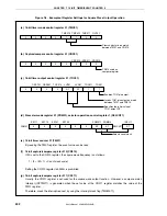
Page 243: ...3 TMC012 bits 00 Register initial setting PRM01 register SELCNT1 register CRC01 register TOC01 registerNote CR010 register port setting Initial setting of these registers is performed before setting the TMC013 and TMC012 bits to 11 Starts count operation The counter is initialized and counting is stopped by clearing the TMC013 and TMC012 bits to 00 START STOP 1 Count operation start flow 2 Count o...

Page 244: ... of times of detection of valid edge of external event Set value of the CR010 register 1 However the first match interrupt immediately after the timer event counter has started operating is generated with the following timing Number of times of detection of valid edge of external event input Set value of the CR010 register 2 To detect the valid edge the signal input to the TI010 pin is sampled dur...

Page 245: ...erts TO01 output on match between TM01 and CR010 CR011 Specifies initial value of TO01 output F F 0 1 0 1 0 1 d Prescaler mode register 01 PRM01 selector operation control register 1 SELCNT1 0 PRM01 0 0 1 0 1 0 PRM011 PRM010 ISEL11 ES111 ES110 ES101 ES100 Selects count clock specifies valid edge of TI010 00 Falling edge detection 01 Rising edge detection 10 Setting prohibited 11 Both edges detecti...

Page 246: ...Register initial setting PRM01 register SELCNT1 register CRC01 register TOC01 registerNote CR010 register port setting Initial setting of these registers is performed before setting the TMC013 and TMC012 bits to 11 Starts count operation The counter is initialized and counting is stopped by clearing the TMC013 and TMC012 bits to 00 START STOP 1 Count operation start flow 2 Count operation stop flo...

Page 247: ...011 registers are used as compare registers Signals INTTM010 and INTTM011 are generated when the value of the TM01 register matches the value of the CR010 and CR011 registers b When the CR010 and CR011 registers are used as capture registers The count value of the TM01 register is captured to the CR010 register and the INTTM010 signal is generated when the valid edge is input to the TI011 pin or w...

Page 248: ...register Figure 7 13 Block Diagram of Clear Start Mode Entered by TI010 Pin Valid Edge Input CR010 register Compare Register CR011 register Compare Register 16 bit counter TM01 Clear Output controller Edge detection Compare register CR011 Match signal TO01 pin Match signal Interrupt signal INTTM010 Interrupt signal INTTM011 TI010 pin Compare register CR010 Operable bits TMC013 TMC012 Count clock ...

Page 249: ...011 TO01 pin output M 10 M N N N N M M M 00 N b TOC01 13H PRM01 10H CRC01 00H TMC01 0AH TM01 register 0000H Operable bits TMC013 TMC012 Count clear input TI010 pin input Compare register CR010 Compare match interrupt INTTM010 Compare register CR011 Compare match interrupt INTTM011 TO01 pin output M 10 M N N N N M M M 00 N a and b differ as follows depending on the setting of the TMC01 register TMC...

Page 250: ...egister Figure 7 15 Block Diagram of Clear Start Mode Entered by TI010 Pin Valid Edge Input CR010 Register Compare Register CR011 Register Capture Register 16 bit counter TM01 Clear Output controller Edge detector Capture register CR011 Capture signal TO01 pin Match signal Interrupt signal INTTM010 Interrupt signal INTTM011 TI010 pin Compare register CR010 Operable bits TMC013 TMC012 Count clock ...

Page 251: ... register CR010 Compare match interrupt INTTM010 Capture register CR011 Capture interrupt INTTM011 TO01 pin output 0000H 10 Q P N M S 00 0000H M N S P Q This is an application example where the output level of the TO01 pin is inverted when the count value has been captured cleared The count value is captured to the CR011 register and the TM01 register is cleared to 0000H when the valid edge of the...

Page 252: ...M011 TO01 pin output 0003H 0003H 10 Q P N M S 00 0000H M 4 4 4 4 N S P Q This is an application example where the width set to the CR010 register 4 clocks in this example is to be output from the TO01 pin when the count value has been captured cleared The count value is captured to the CR011 register a capture interrupt signal INTTM011 is generated the TM01 register is cleared to 0000H and the out...

Page 253: ...egister Figure 7 17 Block Diagram of Clear Start Mode Entered by TI010 Pin Valid Edge Input CR010 Register Capture Register CR011 Register Compare Register 16 bit counter TM01 Clear Output controller Edge detection Capture register CR010 Capture signal TO01 pin Match signal Interrupt signal INTTM011 Interrupt signal INTTM010 TI010 pin Compare register CR011 Operable bits TMC013 TMC012 Count clock ...

Page 254: ...h interrupt INTTM011 TO01 pin output This is an application example where the output level of the TO01 pin is to be inverted when the count value has been captured cleared The TM01 register is cleared at the rising edge detection of the TI010 pin and it is captured to the CR010 register at the falling edge detection of the TI010 pin When the CRC01 CRC011 bit is set to 1 the count value of the TM01...

Page 255: ... is to be output from the TO01 pin when the count value has been captured cleared The TM01 register is cleared to 0000H at the rising edge detection of the TI010 pin and captured to the CR010 register at the falling edge detection of the TI010 pin The output level of the TO01 pin is inverted when the TM01 register is cleared to 0000H because the rising edge of the TI010 pin has been detected or wh...

Page 256: ...I011 pin Selector Figure 7 20 Timing Example of Clear Start Mode Entered by TI010 Pin Valid Edge Input CR010 Register Capture Register CR011 Register Capture Register 1 3 a TOC01 13H PRM01 30H CRC01 05H TMC01 0AH TM01 register 0000H Operable bits TMC013 TMC012 Capture count clear input TI010 pin input Capture register CR010 Capture interrupt INTTM010 Capture register CR011 Capture interrupt INTTM0...

Page 257: ...I011 pin input Capture register CR010 Capture interrupt INTTM010 Capture count clear input TI010 Capture register CR011 Capture interrupt INTTM011 TO01 pin output 10 R S T O L M N P Q 00 FFFFH L L L 0000H 0000H L M N O P Q R S T This is a timing example where an edge is not input to the TI010 pin in an application where the count value is captured to the CR010 register when the rising or falling e...

Page 258: ...o the CR010 register in the phase reverse to the falling edge of the TI010 pin i e rising edge and to the CR011 register at the falling edge of the TI010 pin The high and low level widths of the input pulse can be calculated by the following expressions High level width CR011 register value CR010 register value Count clock cycle Low level width CR010 register value Count clock cycle If the reverse...

Page 259: ...0 1 CRC012 CRC011 CRC010 0 CR010 used as compare register 1 CR010 used as capture register 0 CR011 used as compare register 1 CR011 used as capture register 0 TI011 pin is used as capture trigger of CR010 1 Reverse phase of TI010 pin is used as capture trigger of CR010 c 16 bit timer output control register 01 TOC01 0 0 0 0 1 0 1 LVR01 LVS01 TOC014 OSPE01 OSPT01 TOC011 TOE01 0 Disables TO01 output...

Page 260: ...e compare register 010 CR010 When this register is used as a compare register and when its value matches the count value of the TM01 register an interrupt signal INTTM010 is generated The count value of the TM01 register is not cleared To use this register as a capture register select either the TI010 or TI011 pin input as a capture trigger When the valid edge of the capture trigger is detected th...

Page 261: ...l setting PRM01 register SELCNT1 register CRC01 register TOC01 registerNote CR010 CR011 registers TMC01 TMC011 bit port setting Initial setting of these registers is performed before setting the TMC013 and TMC012 bits to 10 Starts count operation When the valid edge is input to the TI010 pin the value of the TM01 register is cleared START 1 Count operation start flow 2 TM01 register clear start fl...

Page 262: ...ither the CR010 register or CR011 register is used as a compare register and the other is used as a capture register Both the CR010 and CR011 registers are used as capture registers Remarks 1 For the alternate function pin TO01 settings refer to Table 4 12 Settings When Port Pins Are Used for Alternate Functions 2 For enabling the INTTM010 and INTTM011 interrupts refer to CHAPTER 17 INTERRUPT EXCE...

Page 263: ...wo compare registers are used in the free running timer mode The output level of the TO01 pin is reversed each time the count value of the TM01 register matches the set values of the CR010 and CR011 registers When the count value matches the register value the INTTM010 or INTTM011 signal is generated 2 Free running timer mode operation CR010 register compare register CR011 register capture registe...

Page 264: ...pture interrupt INTTM011 TO01 pin output Overflow flag OVF01 0 write clear 0 write clear 0 write clear 0 write clear This is an application example where a compare register and a capture register are used at the same time in the free running timer mode In this example the INTTM010 signal is generated and the output level of the TO01 pin is reversed each time the count value of the TM01 register ma...

Page 265: ... TM01 Capture register CR010 Capture signal Capture signal Interrupt signal INTTM011 Interrupt signal INTTM010 Capture register CR011 Operable bits TMC013 TMC012 Count clock Edge detection TI010 pin Edge detection TI011 pin Selector Remark If both the CR010 and CR011 registers are used as capture registers in the free running timer mode the output level of the TO01 pin is not inverted However it c...

Page 266: ...e register CR011 Capture interrupt INTTM011 Capture trigger input TI011 Capture register CR010 Capture interrupt INTTM010 Overflow flag OVF01 0 write clear 0 write clear 0 write clear 0 write clear This is an application example where the count values that have been captured at the valid edges of separate capture trigger signals are stored in separate capture registers in the free running timer mo...

Page 267: ...ster CR010 Capture interrupt INTTM010 Capture trigger input TI010 Capture register CR011 Capture interrupt INTTM011 01 L M P S N O R Q T 00 0000H 0000H L M N O P Q R S T L L This is an application example where both the edges of the TI011 pin are detected and the count value is captured to the CR010 register in the free running timer mode When both the CR010 and CR011 registers are used as capture...

Page 268: ...0 CR010 used as compare register 1 CR010 used as capture register 0 CR011 used as compare register 1 CR011 used as capture register 0 TI011 pin is used as capture trigger of CR010 1 Reverse phase of TI010 pin is used as capture trigger of CR010 c 16 bit timer output control register 01 TOC01 0 0 0 0 1 0 1 LVR01 LVS01 TOC014 OSPE01 OSPT01 TOC011 TOE01 0 Disables TO01 output 1 Enables TO01 output 00...

Page 269: ...er 010 CR010 When this register is used as a compare register and when its value matches the count value of the TM01 register an interrupt signal INTTM010 is generated The count value of the TM01 register is not cleared To use this register as a capture register select either the TI010 or TI011 pin input as a capture trigger When the valid edge of the capture trigger is detected the count value of...

Page 270: ...MC013 TMC012 bits 0 1 Register initial setting PRM01 register SELCNT1 register CRC01 register TOC01 registerNote CR010 CR011 register TMC01 TMC011 bit port setting Initial setting of these registers is performed before setting the TMC013 and TMC012 bits to 01 Starts count operation START 1 Count operation start flow TMC013 TMC012 bits 0 0 The counter is initialized and counting is stopped by clear...

Page 271: ...egister 1 Count clock cycle Duty Set value of the CR011 register 1 Set value of the CR010 register 1 Caution To change the duty factor value of the CR011 register during operation refer to 7 5 1 Rewriting CR011 register during TM01 operation Remarks 1 For the alternate function pin settings refer to Table 4 12 Settings When Port Pins Are Used for Alternate Functions 2 For enabling the INTTM010 and...

Page 272: ...CR011 00 Disables one shot pulse output Specifies initial value of TO01 output F F 0 1 1 1 d Prescaler mode register 01 PRM01 selector operation control register 1 SELCNT1 0 PRM01 0 0 0 0 PRM011 PRM010 ISEL11 ES111 ES110 ES101 ES100 Selects count clock 0 0 1 0 1 0 1 SELCNT1 e 16 bit timer counter 01 TM01 By reading the TM01 register the count value can be read f 16 bit capture compare register 010...
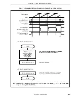
Page 273: ...itial setting PRM01 register SELCNT1 register CRC01 register TOC01 registerNote CR010 CR011 registers port setting Initial setting of these registers is performed before setting the TMC013 and TMC012 bits Starts count operation START 1 Count operation start flow TMC013 TMC012 bits 00 The counter is initialized and counting is stopped by clearing the TMC013 and TMC012 bits to 00 STOP 2 Count operat...

Page 274: ...ion Do not input the trigger again setting OSPT01 to 1 or detecting the valid edge of the TI010 pin while the one shot pulse is output To output the one shot pulse again generate the trigger after the current one shot pulse output has completed Remarks 1 For the alternate function pin settings refer to Table 4 12 Settings When Port Pins Are Used for Alternate Functions 2 For enabling the INTTM010 ...

Page 275: ...d as compare register CR011 used as compare register c 16 bit timer output control register 01 TOC01 0 0 1 1 1 0 1 LVR01 LVS01 TOC014 OSPE01 OSPT01 TOC011 TOE01 Enables TO01 pin output Inverts TO01 output on match between TM01 and CR010 CR011 Specifies initial value of TO01 pin output Enables one shot pulse output Software trigger is generated by writing 1 to this bit operation is not affected eve...

Page 276: ...used as a compare register when a one shot pulse is output When the value of the TM01 register matches that of the CR010 register an interrupt signal INTTM010 is generated and the output level of the TO01 pin is inverted g 16 bit capture compare register 011 CR011 This register is used as a compare register when a one shot pulse is output When the value of the TM01 register matches that of the CR0...

Page 277: ...t TI010 pin Overflow plug OVF01 Compare register CR010 Compare match interrupt INTTM010 Compare register CR011 Compare match interrupt INTTM011 TO01 pin output TO01 output control bits TOE01 TOC014 TOC011 N M N M N M 01 or 10 00 00 N N N M M M M 1 M 1 1 2 2 3 TO01 output level is not inverted because no one shot trigger is input Time from when the one shot pulse trigger is input until the one shot...

Page 278: ...isters is performed before setting the TMC013 and TMC012 bits Starts count operation START 1 Count operation start flow 2 One shot trigger input flow TMC013 TMC012 bits 00 The counter is initialized and counting is stopped by clearing the TMC013 and TMC012 bits to 00 STOP 3 Count operation stop flow TOC01 OSPT01 bit 1 or edge input to TI010 pin Write the same value to the bits other than the OSPT0...

Page 279: ...01 flag If it is set to 1 clear it to 0 by software Figure 7 37 Block Diagram of Pulse Width Measurement Free Running Timer Mode 16 bit counter TM01 Capture register CR010 Capture signal Capture signal Interrupt signal INTTM011 Interrupt signal INTTM010 Capture register CR011 Operable bits TMC013 TMC012 Count clock Edge detection TI010 pin Edge detection TI011 pin Selector Figure 7 38 Block Diagra...

Page 280: ...s captured to the CR011 register When the valid edge of the TI011 pin is detected the count value of the TM01 register is captured to the CR010 register Specify detection of both the edges of the TI010 and TI011 pins By this measurement method the previous count value is subtracted from the count value captured by the edge of each input signal Therefore save the previously captured value to a sepa...

Page 281: ...ave to be saved By subtracting the value of one capture register from that of another a high level width low level width and cycle are calculated If an overflow occurs the value becomes negative if one captured value is simply subtracted from another and therefore a borrow occurs the PSW CY bit is set to 1 If this happens ignore CY and take the calculated value as the pulse width In addition clear...

Page 282: ...verflow If an overflow occurs take the value that results from adding 10000H to the value stored in the CR011 register as a cycle Clear the TMC01 OVF01 bit to 0 Figure 7 41 Timing Example of Pulse Width Measurement 3 TMC01 08H PRM01 10H CRC01 07H FFFFH TM01 register 0000H Operable bits TMC013 TMC012 Capture count clear input TI010 Capture register CR010 Capture register CR011 Capture interrupt INT...

Page 283: ...I011 pin is used as capture trigger of CR010 1 Reverse phase of TI010 pin is used as capture trigger of CR010 c 16 bit timer output control register 01 TOC01 0 0 0 0 0 LVR01 LVS01 TOC014 OSPE01 OSPT01 TOC011 TOE01 0 0 0 d Prescaler mode register 01 PRM01 selector operation control register 1 SELCNT1 Selects count clock setting valid edge of TI010 is prohibited 00 Falling edge detection 01 Rising e...

Page 284: ...his register is used as a capture register Either the TI010 or TI011 pin is selected as a capture trigger When a specified edge of the capture trigger is detected the count value of the TM01 register is stored in the CR010 register g 16 bit capture compare register 011 CR011 This register is used as a capture register The signal input to the TI010 pin is used as a capture trigger When the capture ...

Page 285: ...gger input TI011 Capture register CR010 Capture interrupt INTTM010 01 D00 D00 D01 D01 D02 D02 D03 D03 D04 D04 D10 D10 D11 D11 D12 D12 D13 D13 00 00 0000H 0000H 1 2 2 2 2 2 2 2 2 2 3 b Example of clear start mode entered by TI010 pin valid edge FFFFH TM01 register 0000H Operable bits TMC013 TMC012 Capture count clear input TI010 Capture register CR010 Capture interrupt INTTM010 Capture register CR0...

Page 286: ...or 10 Register initial setting PRM01 register SELCNT1 register CRC01 register port setting Initial setting of these registers is performed before setting the TMC013 and TMC012 bits Starts count operation START 1 Count operation start flow TMC013 TMC012 bits 00 The counter is initialized and counting is stopped by clearing the TMC013 and TMC012 bits to 00 STOP 3 Count operation stop flow Note The c...

Page 287: ...K11 bit 1 2 Disable reversal of the timer output when the value of the TM01 register matches that of the CR011 register TOC01 TOC014 bit 0 3 Change the value of the CR011 register 4 Wait for one cycle of the count clock of the TM01 register 5 Enable reversal of the timer output when the value of the TM01 register matches that of the CR011 register TOC01 TOC014 bit 1 6 Clear the interrupt flag of I...

Page 288: ...1 Bits TOC01 LVS01 bit TOC01 LVR01 bit Operable bits TMC013 TMC012 TO01 pin output INTTM010 signal 1 00 2 1 3 4 4 4 01 10 or 11 1 The TO01 pin output goes high when the LVS01 and LVR01 bits 10 2 The TO01 pin output goes low when the LVS01 and LVR01 bits 01 the pin output remains unchanged from the high level even if the LVS01 and LVR01 bits are cleared to 00 3 The timer starts operating when the T...

Page 289: ...e TI010 pin input use the output of the TO01 pin that functions alternately as P32 When using the output of the TO01 pin that functions alternately as P35 the TI010 pin that functions alternately as P35 cannot be used Therefore the TO01 pin output inversion operation by detecting the valid edge of the TI010 pin input cannot be performed When using the TO01 pin that functions alternately as P35 cle...

Page 290: ...lse TM01 count value Edge input INTTM011 Value captured to CR011 Capture read signal Capture operation is performed but read value is not guaranteed Capture operation b The values of the CR010 and CR011 registers are not guaranteed after 16 bit timer event counter 01 has stopped 5 Setting valid edge Set the valid edge of the TI010 pin while the timer operation is stopped TMC01 TMC013 and TMC01 TMC...

Page 291: ...ster Figure 7 48 Operation Timing of OVF01 Flag FFFEH FFFFH FFFFH 0000H 0001H Count pulse TM01 INTTM010 OVF01 CR010 b Clearing of OVF01 flag After the TM01 register overflows clearing OVF01 flag is invalid and set 1 again even if the OVF01 flag is cleared 0 before the next count clock is counted before TM01 register becomes 0001H 8 One shot pulse output One shot pulse output operates normally in e...

Page 292: ...011 pin during this operation the capture operation is not performed but the INTTM010 signal is generated as an external interrupt signal Mask the INTTM010 signal when the external interrupt is not used 10 Edge detection a Specifying valid edge after reset If the operation of the 16 bit timer event counter 01 is enabled after reset and while the TI010 or TI011 pin is at high level and when the ris...

Page 293: ... Mode using 8 bit timer event counter alone individual mode 8 bit timer event counter 5n operates as an 8 bit timer event counter The following functions can be used Interval timer External event counter Square wave output PWM output 2 Mode using cascade connection 16 bit resolution cascade connection mode 8 bit timer event counter 5n operates as a 16 bit timer event counter by connecting the TM50...

Page 294: ...1 TMC50 TMC51 16 bit timer mode control register 5 TMC5 Only when using cascade connection Note When using the functions of the TI5n and TO5n pins refer to Table 4 12 Settings When Port Pins Are Used for Alternate Functions Remark n 0 1 The block diagram of 8 bit timer event counter 5n is shown below Figure 8 1 Block Diagram of 8 Bit Timer Event Counter 5n OVF TI5n 3 TCL5n2 TCL5n1 TCL5n0 TCE5nTMC5...

Page 295: ...ers can be read only in 16 bit units Therefore read these registers twice and compare the values taking into consideration that the reading occurs during a count change TM5n n 0 1 6 4 2 After reset 00H R Address TM50 FFFFF5C0H TM51 FFFFF5C1H 0 7 5 3 1 The count value is reset to 00H in the following cases 1 Reset 2 When the TMC5n TCE5n bit is cleared 0 3 The TM5n register and CR5n register match i...

Page 296: ...00H to FFH When using the TM50 register and TM51 register in cascade as a 16 bit timer the CR50 register and CR51 register operate as 16 bit timer compare register 5 CR5 The counter value and register value are compared in 16 bit lengths and if they match an interrupt request signal INTTM50 is generated CR5n n 0 1 6 4 2 After reset 00H R W Address CR50 FFFFF5C2H CR51 FFFFF5C3H 0 7 5 3 1 Cautions 1...

Page 297: ...ts Reset sets this register to 00H Falling edge of TI5n Rising edge of TI5n fXX fXX 2 fXX 4 fXX 64 fXX 256 INTTM010 Count clock selectionNote TCL5n2 0 0 0 0 1 1 1 1 TCL5n1 0 0 1 1 0 0 1 1 TCL5n0 0 1 0 1 0 1 0 1 20 MHz 10 MHz Setting prohibited 100 ns 200 ns 3 2 s 12 8 s 100 ns 200 ns 0 4 s 6 4 s 25 6 s Clock fXX 0 TCL5n n 0 1 0 0 0 0 TCL5n2 TCL5n1 TCL5n0 After reset 00H R W Address TCL50 FFFFF5C4H...

Page 298: ... by the TM5n register Selects the operation mode of the TM5n register Selects the individual mode or cascade connection mode Sets the status of the timer output flip flop Controls the timer output flip flop or selects the active level in the PWM free running timer mode Controls timer output The TMC5n register can be read or written in 8 bit or 1 bit units Reset sets this register to 00H ...

Page 299: ...operation Enable inversion operation High active Low active TMC5n1 0 1 Other than PWM free running timer mode TMC5n6 bit 0 Controls timer F F PWM free running timer mode TMC5n6 bit 1 Selects active level Disable output TO5n pin is low level Enable output TOE5n 0 1 Timer output control 7 6 5 4 3 2 1 0 Note Bit 4 of the TMC50 register is fixed to 0 Cautions 1 Because the TO51 and TI51 pins are alter...

Page 300: ...ion and selects the mode in which clear start occurs on a match between the TM5n register and CR5n register TMC5n register 0000xx00B don t care 2 When the TMC5n TCE5n bit is set to 1 the count operation starts 3 When the values of the TM5n register and CR5n register match the INTTM5n signal is generated TM5n register is cleared to 00H 4 Then the INTTM5n signal is repeatedly generated at the same i...

Page 301: ...2 2 When CR5n register 00H t Interval time 00H 00H 00H 00H 00H Count clock TM5n count value CR5n TCE5n INTTM5n Remark n 0 1 When CR5n register FFH t 01H 00H FEH FFH 00H FEH FFH 00H FFH FFH FFH Count clock TM5n count value CR5n TCE5n INTTM5n Interval time Interrupt acknowledgment Interrupt acknowledgment Remark n 0 1 ...

Page 302: ...ts the mode in which clear start occurs on a match between the TM5n register and CR5n register disables timer output F F inversion operation and disables timer output TMC5n register 0000xx00B don t care For the alternate function pin settings refer to Table 4 12 Settings When Port Pins Are Used for Alternate Functions 2 When the TMC5n TCE5n bit is set to 1 the counter counts the number of pulses i...

Page 303: ...mode in which clear start occurs on a match between the TM5n register and CR5n register sets initial value of timer output enables timer output F F inversion operation and enables timer output TMC5n register 00001011B or 00000111B For the alternate function pin settings refer to Table 4 12 Settings When Port Pins Are Used for Alternate Functions 2 When the TMC5n TCE5n bit is set to 1 counting star...

Page 304: ...tion t Interval time Interval time 00H N 01H 01H 00H N N N N N N 01H 00H Clear Interrupt acknowledgment Interrupt acknowledgment Clear Count clock TM5n count value CR5n TO5nNote TCE5n INTTM5n Count start Note The initial value of the TO5n pin output can be set using the TMC5n LVS5n and TMC5n LVR5n bits Remark n 0 1 ...

Page 305: ...r 01000001B or 01000011B For the alternate function pin settings refer to Table 4 12 Settings When Port Pins Are Used for Alternate Functions 2 When the TMC5n TCE5n bit is set to 1 counting starts PWM output operation 1 When counting starts PWM output output from the TO5n pin outputs the inactive level until an overflow occurs 2 When an overflow occurs the active level set by setting method 1 is o...

Page 306: ...l Active level Count clock TM5n count value CR5n TCE5n INTTM5n TO5n t When CR5n register 00H 00H N 1N 2 N 00H 00H M 00H FFH 01H 02H 01H 00H FFH 02H 01H Inactive level Inactive level Count clock TM5n count value CR5n TCE5n INTTM5n TO5n t When CR5n register FFH 00H N 1N 2 N FFH 00H M 00H FFH 01H 02H 01H 00H FFH 02H 01H Inactive level Inactive level Inactive level Active level Active level Count cloc...

Page 307: ...ition N M M M 1M 2 M M 1M 2 FFH 02H 00H 01H FFH 02H 00H 01H Count clock TM5n count value CR5n TCE5n H INTTM5n TO5n 2 t When the value of the CR5n register changes from N to M after the rising edge of the FFH clock The value of the CR5n register is transferred at the second overflow N N 1 N 2 N N N 1 CR5n transition N M M N 1 N 2 M M 1M 2 FFH 03H 02H 00H 01H FFH 02H 00H 01H Count clock TM5n count v...

Page 308: ...e TMC50 register 0000xx00B TMC51 register 0001xx00B 2 Set the TMC51 TCE51 bit to 1 Then set the TMC50 TCE50 bit to 1 to start the count operation 3 When the values of the TM5 register and CR5 register connected in cascade match the INTTM50 signal is generated the TM5 register is cleared to 0000H 4 The INTTM50 signal is then generated repeatedly at the same interval Interval time N 1 t N 0000H to F...

Page 309: ...16 bit resolution Figure 8 7 Cascade Connection Mode with 16 Bit Resolution 00H N 1 01H 00H FFH 00H 01H FFH 00H FFH M 1 01H 00H 00H N A 01H 00H 02H M 00H 00H B N N M Interval time Operation enabled count start Interrupt occurrence counter cleared Operation stopped Count clock TM50 count value TM51 count value TCE51 INTTM50 CR51 TCE50 CR50 t ...

Page 310: ...ettings refer to Table 4 12 Settings When Port Pins Are Used for Alternate Functions 2 Set the TMC51 TCE51 bit to 1 Then set the TMC50 TCE50 bit to 1 and count the number of pulses input from the TI50 pin 3 When the values of the TM5 register and CR5 register connected in cascade match the INTTM50 signal is generated the TM5 register is cleared to 0000H 4 The INTTM50 signal is then generated each ...

Page 311: ...t occurs on a match between the TM5 register and CR5 register LVS50 LVR50 Timer Output F F Status Settings 1 0 High level output 0 1 Low level output Enables timer output F F inversion and enables timer output TMC50 register 00001011B or 00000111B TMC51 register 00010000B For the alternate function pin settings refer to Table 4 12 Settings When Port Pins Are Used for Alternate Functions 2 Set the ...

Page 312: ...imer An error of up to 1 clock occurs before the match signal is generated after the timer has been started This is because the TM5n register is started asynchronously to the count pulse Figure 8 8 Count Start Timing of TM5n Register 00H Timer start 01H 02H 03H 04H Count pulse TM5n count value Remark n 0 1 ...

Page 313: ... following hardware Table 9 1 Configuration of 8 Bit Timer Hn Item Configuration Timer registers 8 bit timer counter Hn 1 each Registers 8 bit timer H compare register n0 CMPn0 1 each 8 bit timer H compare register n1 CMPn1 1 each Timer outputs TOHn output controller Control registers Note 8 bit timer H mode register n TMHMDn 8 bit timer H carrier control register n TMCYCn Note To use the TOHn pin...

Page 314: ...mode register n TMHMDn 8 bit timer H carrier control register n TMCYCn Note fXX 2 10 when n 0 fR 2 11 when n 1 Remark n 0 1 1 8 bit timer H compare register n0 CMPn0 This CMPn0 register can be read or written in 8 bit units This register is used in all of the timer operation modes This register constantly compares the value set to the CMPn0 register with the count value of 8 bit timer counter Hn a...

Page 315: ...value of the CMPn1 register is changed to the new value If matching of the count value and the CMPn1 register value and writing a value to the CMPn1 register conflict the value of the CMPn1 register is not changed Reset sets this register to 00H CMPn1 n 0 1 After reset 00H R W Address CMP01 FFFFF583H CMP11 FFFFF593H 7 6 5 4 3 2 1 0 The CMPn1 register can be rewritten during timer count operation I...

Page 316: ...timer H carrier control register n TMCYCn Remarks 1 To use the TOHn pin function refer to Table 4 12 Settings When Port Pins Are Used for Alternate Functions 2 n 0 1 1 8 bit timer H mode register n TMHMDn The TMHMDn register controls the mode of 8 bit timer Hn The TMHMDn register can be read or written in 8 bit or 1 bit units Reset sets this register to 00H Remark n 0 1 ...

Page 317: ... 1 Timer output level control default Disable output Enable output TOEN0 0 1 Timer output control fXX 16 0 MHz 7 6 5 4 3 2 1 0 μ μ μ Setting prohibited fXX 10 0 MHz Setting prohibited 100 ns 200 ns 800 ns 3 2 s 51 2 s fXX 20 MHz μ μ 100 ns 200 ns 400 ns 1 6 s 6 4 s 102 4 s μ μ μ Note Set so as to satisfy the following conditions VDD 4 0 to 5 5 V Count clock 10 MHz VDD 2 7 to 4 0 V Count clock 5 MH...

Page 318: ... level High level TOLEV1 0 1 Timer output level control default Disable output Enable output TOEN1 0 1 Timer output control fXX 16 0 MHz 7 6 5 4 3 2 1 0 μ μ Setting prohibited 100 ns 200 ns 800 ns 3 2 s fXX 20 0 MHz fXX 10 0 MHz 100 ns 200 ns 400 ns 1 6 s 6 4 s μ μ μ Note Set so as to satisfy the following conditions VDD 4 0 to 5 5 V Count clock 10 MHz VDD 2 7 to 4 0 V Count clock 5 MHz Cautions 1...

Page 319: ... in 8 bit or 1 bit units The NRZn bit is a read only bit Reset sets this register to 00H 0 TMCYCn n 0 1 0 0 0 0 RMCn NRZBn NRZn After reset 00H R W Address TMCYC0 FFFFF581H TMCYC1 FFFFF591H Low level output High level output Low level output Carrier pulse output RMCn 0 0 1 1 NRZBn 0 1 0 1 Remote control output Carrier output disabled status low level status Carrier output enable status NRZn 0 1 Ca...

Page 320: ...s When Port Pins Are Used for Alternate Functions 2 For INTTMHn interrupt enable refer to CHAPTER 17 INTERRUPT EXCEPTION PROCESSING FUNCTION Setting 1 Set each register Figure 9 2 Register Settings in Interval Timer Mode i 8 bit timer H mode register n TMHMDn settings 0 0 1 0 1 0 1 0 Sets timer output Sets timer output default level Sets interval timer mode Selects count clock fCNT Stops count ope...

Page 321: ... the TMHEn bit is set to 1 the count operation is enabled The count clock starts counting no more than one clock after operation has been enabled 2 When the count value of 8 bit timer counter Hn and the set value of the CMPn0 register match the value of 8 bit timer counter Hn is cleared the TOHn output level is inverted and the INTTMHn signal is output at the rising edge of the count clock 3 The I...

Page 322: ...ister FFH 00H CMPn0 TMHEn INTTMHn TOHn 01H FEH FFH 00H FEH FFH 00H FFH Interval time Count clock Count start Clear Clear 8 bit timer counter Hn count value Operation when CMPn0 register 00H Count clock Count start CMPn0 TMHEn INTTMHnNote TOHn 00H 00H 8 bit timer counter Hn count value Note The INTTMHn interrupt is generated only once Remark n 0 1 R ...

Page 323: ...ue of 8 bit timer counter Hn and the set value of the CMPn1 register match the TOHn output level is inverted Remarks 1 For the alternate function pin TOHn settings refer to Table 4 12 Settings When Port Pins Are Used for Alternate Functions 2 For INTTMHn interrupt enable refer to CHAPTER 17 INTERRUPT EXCEPTION PROCESSING FUNCTION Setting 1 Set each register Figure 9 4 Register Settings in PWM Outp...

Page 324: ...e of any duty can be obtained through the repetition of steps 3 and 4 above 6 To stop the count operation clear the TMHEn bit to 0 Designating the set value of the CMPn0 register as N the set value of the CMPn1 register as M and the count clock frequency as fCNT the PWM pulse output cycle and duty are as follows PWM pulse output cycle N 1 fCNT Duty Inactive width Active width M 1 N 1 Cautions 1 Th...

Page 325: ...lt level 2 When the count value of 8 bit timer counter Hn and the set value of the CMPn0 register match the TOHn output level is inverted 8 bit timer counter Hn is cleared and the INTTMHn signal is output 3 When the count value of 8 bit timer counter Hn and the set value of the CMPn1 register match the TOHn output level is inverted At this time the value of 8 bit timer counter Hn is not cleared an...

Page 326: ...0H Count clock CMPn0 TMHEn INTTMHn TOHn TOLEVn 0 00H 01H FFH 00H 01H 02H FFH 00H FFH 00H 01H 02H CMPn1 FFH 00H 8 bit timer counter Hn count value Operation when CMPn0 register FFH CMPn1 register FEH Count clock CMPn0 TMHEn INTTMHn TOHn TOLEVn 0 00H 01H FEH FFH 00H 01H FEH FFH 00H 01H FEH FFH 00H CMPn1 FFH FEH 8 bit timer counter Hn count value Remark n 0 1 ...

Page 327: ... 327 Figure 9 5 Operation Timing in PWM Output Mode 3 4 Operation when CMPn0 register 01H CMPn1 register 00H Count clock CMPn0 TMHEn INTTMHn TOHn TOLEVn 0 01H 00H 01H 00H 01H 00H 00H 01H 00H 01H CMPn1 00H 8 bit timer counter Hn count value Remark n 0 1 ...

Page 328: ...and the INTTMHn signal is generated 4 Even if the value of the CMPn1 register is changed that value is latched and not transferred to the register When the count value of 8 bit timer counter Hn and the set value of the CMPn1 register prior to the change match the changed value is transferred to the CMPn1 register and the value of the CMPn1 register is changed 2 However three or more count clocks a...

Page 329: ... enable refer to CHAPTER 17 INTERRUPT EXCEPTION PROCESSING FUNCTION 1 Carrier generation In the carrier generator mode the CMPn0 register generates a waveform with the low level width of the carrier pulse and the CMPn1 register generates a waveform with the high level width of the carrier pulse During 8 bit timer Hn operation the CMPn1 register can be rewritten but rewriting of the CMPn0 register ...

Page 330: ...TM5n signal is synchronized with the count clock of 8 bit timer Hn and is output as the INTTM5Hn signal 2 The value of the NRZBn bit is transferred to the NRZn bit at the second clock from the rising edge of the INTTM5Hn signal 3 Write the next value to the NRZBn bit in the interrupt servicing programming that has been started by the INTTM5Hn interrupt or after timing has been checked by polling t...

Page 331: ...er Hn is cleared and at the same time the register that is compared with 8 bit timer counter Hn changes from the CMPn0 register to the CMPn1 register 5 When the count value of 8 bit timer counter Hn and the set value of the CMPn1 register match the INTTMHn signal is generated 8 bit timer counter Hn is cleared and at the same time the register that is compared with 8 bit timer counter Hn changes fr...

Page 332: ...operation was stopped TMHEn bit 0 be sure to set again even if setting the same value to the CMPn1 register 2 Set the values of the CMPn0 and CMPn1 registers in the range of 01H to FFH 3 In the carrier generator mode three operating clocks signal selected by the TMHMDn CKSHn0 to TMHMDn CKSHn2 bits are required for actual transfer of the new value to the register after the CMPn1 register has been r...

Page 333: ... register match the first INTTMHn signal is generated the carrier clock signal is inverted and the register that is compared with 8 bit timer counter Hn changes from the CMPn0 register to the CMPn1 register 8 bit timer counter Hn is cleared to 00H 4 When the count value of 8 bit timer counter Hn and the set value of the CMPn1 register match the INTTMHn signal is generated the carrier clock signal ...

Page 334: ... clock signal is inverted and the register that is compared with 8 bit timer counter Hn changes from the CMPn0 register to the CMPn1 register 8 bit timer counter Hn is cleared to 00H 4 When the count value of 8 bit timer counter Hn and the set value of the CMPn1 register match the INTTMHn signal is generated the carrier clock signal is inverted and the register that is compared with 8 bit timer co...

Page 335: ... while the 8 bit timer Hn is operating The new value L to which the value of the register is to be changed is latched When the count value of the 8 bit timer counter Hn matches the value M of the CMPn1 register before the change the CMPn1 register is changed 3 However it takes three count clocks or more since the value of the CMPn1 register has been changed until the value is transferred to the re...

Page 336: ...ated at a specified interval Generation of count clock for watch timer When the main clock is used as the count clock for the watch timer a count clock fBRG is generated 10 1 2 Configuration The following shows the block diagram of interval timer BRG Figure 10 1 Block Diagram of Interval Timer BRG fX fX 8 fX 4 fX 2 fX BGCS0 BGCS1 TODIS BGCE 3 bit prescaler 8 bit counter Clear Match fBGCS Count clo...

Page 337: ... selector selects the count clock fBGCS for interval timer BRG from fX fX 2 fX 4 and fX 8 4 8 bit counter The 8 bit counter counts the count clock fBGCS 5 Output control The output control controls supply of the count clock fBRG for the watch timer 6 PRSCM register The PRSCM register is an 8 bit compare register that sets the interval time 7 PRSM register The PRSM register controls the operation o...

Page 338: ...ion fX fX 2 fX 4 fX 8 5 MHz 200 ns 400 ns 800 ns 1 6 s 4 MHz 250 ns 500 ns 1 s 2 s BGCS1 0 0 1 1 BGCS0 0 1 0 1 Selection of input clock fBGCS Note After reset 00H R W Address FFFFF8B0H Clock for watch timer supplied Clock for watch timer not supplied TODIS 0 1 Control of clock supply for watch timer 10 MHz 100 ns 200 ns 400 ns 800 ns μ μ μ Note Set these bits so that the following conditions are s...

Page 339: ...register This register can be read or written in 8 bit units Reset sets this register to 00H PRSCM7 PRSCM PRSCM6 PRSCM5 PRSCM4 PRSCM3 PRSCM2 PRSCM1 PRSCM0 After reset 00H R W Address FFFFF8B1H Caution Do not rewrite the PRSCM register while interval timer BRG is operating PRSM BGCE bit 1 Set the PRSCM register before setting 1 the BGCE bit ...

Page 340: ...ount clock supply for watch timer Set the count clock by using the PRSM BGCS1 and PRSM BGCS0 bits and the 8 bit compare value by using the PRSCM register so that the count clock frequency fBRG of the watch timer is 32 768 kHz Clear 0 the PRSM TODIS bit at the same time When the PRSM BGCE bit is set 1 fBRG is supplied to the watch timer fBRG is obtained from the following equation fBRG fX 2 m 1 N T...

Page 341: ...functions can be used at the same time 10 2 2 Configuration The following shows the block diagram of the watch timer Figure 10 2 Block Diagram of Watch Timer Internal bus Watch timer operation mode register WTM fBRG fW 24 fW 25 fW 26 fW 27 fW 28 fW 210 fW 211 fW 29 fXT 11 bit prescaler Clear Clear INTWT INTWTI WTM0 WTM1 WTM2 WTM3 WTM4 WTM5 WTM6 WTM7 5 bit counter fW 3 Selector Selector Selector Se...

Page 342: ... the INTWT signal generation time interval Selector that selects the generation time interval of the interval timer WT interrupt request signal INTWTI from 24 fW to 2 11 fW 4 8 bit counter The 8 bit counter counts the count clock fBGCS 5 WTM register The WTM register is an 8 bit register that controls the operation of the watch timer interval timer WT and sets the interval of interrupt request sig...

Page 343: ...M2 WTM1 WTM0 WTM5 0 0 1 1 0 0 1 1 0 0 1 1 0 0 1 1 WTM4 0 1 0 1 0 1 0 1 0 1 0 1 0 1 0 1 After reset 00H R W Address FFFFF680H μ μ μ μ 214 fW 0 5 s fW fXT 213 fW 0 25 s fW fXT 25 fW 977 s fW fXT 24 fW 488 s fW fXT 214 fW 0 5 s fW fBRG 213 fW 0 25 s fW fBRG 25 fW 977 s fW fBRG 24 fW 488 s fW fBRG WTM7 0 0 0 0 1 1 1 1 Selection of watch timer interrupt INTWT time Clear after operation stops Start WTM1...

Page 344: ...unt value set in advance The interval time can be selected by the WTM WTM4 to WTM WTM7 bits Table 10 1 Interval Time of Interval Timer WTM7 WTM6 WTM5 WTM4 Interval Time 0 0 0 0 2 4 1 fW 488 μs operating at fW fXT 32 768 kHz 0 0 0 1 2 5 1 fW 977 μs operating at fW fXT 32 768 kHz 0 0 1 0 2 6 1 fW 1 95 ms operating at fW fXT 32 768 kHz 0 0 1 1 2 7 1 fW 3 91 ms operating at fW fXT 32 768 kHz 0 1 0 0 2...

Page 345: ... s Interrupt time of watch timer 0 5 s Interval time T Interval time T nT nT 5 bit counter Count clock fW or fW 29 Watch timer interrupt INTWT Interval timer interrupt INTWTI Remarks 1 Assuming that the interrupt time of the watch timer is set to 0 5 seconds 2 fW Watch timer clock frequency Values in parentheses apply when count clock fW 32 768 kHz n Number of interval timer WT operations ...

Page 346: ...lue stop operation When using the main clock as the count clock for interval timer WT the interval time of interval timer BRG can be set to any value but cannot be changed later it can be changed only when interval timer WT stops operation The interval time of interval timer WT can be set to 25 to 2 12 of the set value of interval timer BRG It can also be changed later 4 When watch timer and inter...

Page 347: ...e interrupt request signal INTWDT1 upon overflow of watchdog timer 1Note Generation of system reset signal WDTRES1 upon overflow of watchdog timer 1 Generation of maskable interrupt request signal INTWDTM1 upon overflow of interval timer Note For non maskable interrupt servicing due to non maskable interrupt request signal INTWDT1 INTWDT2 refer to 17 10 Cautions Remark Select whether to use watchd...

Page 348: ...14 fXW 213 INTWDT1 fXW Internal bus Watchdog timer mode register 1 WDTM1 Watchdog timer clock selection register WDCS Output controller Prescaler Clear Selector Remark INTWDTM1 Request signal for maskable interrupt through watchdog timer 1 overflow INTWDT1 Request signal for non maskable interrupt through watchdog timer 1 overflow WDTRES1 Reset signal through watchdog timer 1 overflow fXW fX Watch...

Page 349: ...This register sets the overflow time of watchdog timer 1 and the interval timer The WDCS register can be read or written in 8 bit or 1 bit units Reset sets this register to 00H 0 WDCS 0 0 0 0 WDCS2 WDCS1 WDCS0 213 fXW 214 fXW 215 fXW 216 fXW 217 fXW 218 fXW 219 fXW 221 fXW WDCS2 0 0 0 0 1 1 1 1 Overflow time of watchdog timer 1 interval timer WDCS1 0 0 1 1 0 0 1 1 WDCS0 0 1 0 1 0 1 0 1 4 MHz 10 MH...

Page 350: ...lation clock RUN1 Stop counting Clear counter and start counting RUN1 0 1 Selection of operation mode of watchdog timer 1Note 1 WDTM1 0 0 WDTM14 WDTM13 0 0 0 After reset 00H R W Address FFFFF6C2H Interval timer mode Upon overflow maskable interrupt INTWDTM1 is generated Watchdog timer mode 1Note 3 Upon overflow non maskable interrupt INTWDT1 is generated Watchdog timer mode 2 Upon overflow reset o...

Page 351: ...is generated The count operation of watchdog timer 1 stops in the STOP mode and IDLE mode Set the RUN1 bit to 1 before the STOP mode or IDLE mode is entered in order to clear watchdog timer 1 Because watchdog timer 1 operates in the HALT mode make sure that an overflow will not occur during HALT Cautions 1 When the subclock is selected for the CPU clock the count operation of watchdog timer 1 is s...

Page 352: ...erval timer continues to operate in the HALT mode but it stops operating in the STOP mode and the IDLE mode Cautions 1 Once the WDTM14 bit is set to 1 thereby selecting the watchdog timer 1 mode the interval timer mode is not entered as long as reset is not performed 2 When the subclock is selected for the CPU clock the count operation of the watchdog timer 1 stops the value of the watchdog timer ...

Page 353: ...ction or clear once watchdog timer 2 and stop it within the next interval time Also write to the WDTM2 register for verification purposes only once even if the default settings reset mode interval time fXX 2 25 need not be changed 2 For non maskable interrupt servicing due to a non maskable interrupt request signal INTWDT2 refer to 17 10 Cautions Figure 11 2 Block Diagram of Watchdog Timer 2 fR 8 ...

Page 354: ...ils refer to 3 4 8 1 b Access to special on chip peripheral I O register When the CPU operates on the subclock and the main clock oscillation is stopped When the CPU operates on the internal oscillation clock 0 WDTM2 WDM21 WDM20 WDCS24 WDCS23 WDCS22 WDCS21 WDCS20 After reset 67H R W Address FFFFF6D0H Stops operation Non maskable interrupt request mode generation of INTWDT2 Reset mode generation of...

Page 355: ... 500 ms fXT 32 768 kHz 0 1 1 1 0 2 15 fXT 1000 ms fXT 32 768 kHz 0 1 1 1 1 2 16 fXT 2000 ms fXT 32 768 kHz 1 Operation stopped Note For frequency characteristics error of internal oscillation clock fR refer to CHAPTER 28 ELECTRICAL SPECIFICATIONS 2 Watchdog timer enable register WDTE The counter of watchdog timer 2 is cleared and counting restarted by writing ACH to the WDTE register The WDTE regi...

Page 356: ...iting ACH to the WDTE register clears the counter of watchdog timer 2 and starts the count operation again After the count operation starts write ACH to the WDTE register within the set program loop detection time interval If the program loop detection time is exceeded without ACH being written to the WDTE register a reset signal WDTRES2 or non maskable interrupt request signal INTWDT2 is generate...

Page 357: ...able for controlling a stepping motor In the V850ES KE1 a 6 bit real time output port channel is provided The real time output port can be set in the port mode or real time output port mode in 1 bit units The block diagram of RTO is shown below Figure 12 1 Block Diagram of RTO Real time buffer register 0H RTBH0 Real time output latch 0H Selector INTTM50 INTTM51 Real time output latch 0L RTPOE0 RTP...

Page 358: ...ther of these registers Moreover the data of both these registers can be read at once by specifying the address of either of these registers Table 12 2 shows the operation when the RTBL0 and RTBH0 registers are manipulated 0 RTBL0 RTBH0 0 RTBH05 RTBH04 RTBL03 RTBL02 RTBL01 RTBL00 After reset 00H R W Address RTBL0 FFFFF6E0H RTBH0 FFFFF6E2H Cautions 1 When writing to bits 6 and 7 of the RTBH0 regist...

Page 359: ...l time output disabled Real time output enabled Control of real time output port m 0 to 5 RTPM0 0 RTPM05 RTPM04 RTPM03 RTPM02 RTPM01 RTPM00 After reset 00H R W Address FFFFF6E4H Cautions 1 To reflect real time output signals RTPOUT00 to RTPOUT05 to the pins RTP00 to RTP05 set them to the real time output port with the PMC5 and PFC5 registers 2 By enabling real time output operation RTPC0 RTPOE0 bi...

Page 360: ...EXTR0Note 2 0 0 0 0 4 bits 1 channel 2 bits 1 channel 6 bits 1 channel BYTE0 0 1 Specification of channel configuration for real time output After reset 00H R W Address FFFFF6E5H Notes 1 The value of the RTPEG0 bit does not affect the operation 2 For the EXTR0 bit refer to Table 12 3 3 When real time output operation is disabled RTPOE0 bit 0 real time output signals RTPOUT00 to RTPOUT05 all output...

Page 361: ...specified as real time output disabled by the RTPM0 register output 0 If the real time output operation is disabled by clearing the RTPOE0 bit to 0 the RTPOUT00 to RTPOUT05 signals output 0 regardless of the setting of the RTPM0 register Figure 12 2 Example of Operation Timing of RTO0 When EXTR0 and BYTE0 Bits 00 A B A B A B A B D01 D02 D03 D04 D11 D12 D13 D14 D11 D12 D13 D14 D01 D02 D03 D04 INTTM...

Page 362: ...nd RTBL0 registers is performed when the RTPOE0 bit 0 that value is transferred to real time output latches 0H and 0L respectively 2 Even if write is performed to the RTBH0 and RTBL0 registers when the RTPOE0 bit 1 data transfer to real time output latches 0H and 0L is not performed Caution To reflect the real time output signals RTPOUT00 to RTPOUT05 to the pins set the real time output ports RTP0...

Page 363: ...placed in high impedance by INTP0Note 1 pin are initialized Note 2 so settings for these ports must be performed again Notes 1 Regardless of the port settings P50 to P55 pins are all placed in high impedance via the INTP0 pin 2 The bits that are initialized are all the bits corresponding to P50 to P55 pins of the following registers P5 register PM5 register PMC5 register PU5 register PFC5 register...

Page 364: ...1H R W Address FFFFF806H Note For details on the SELPLL and PLLON bits refer to CHAPTER 5 CLOCK GENERATION FUNCTION Cautions 1 Before outputting a value to the real time output ports RTP00 to RTP05 select the INTP0 pin interrupt edge detection and then set the RTOST0 bit 2 To set again the ports P50 to P55 pins as real time output ports after placing them in high impedance via the INTP0 pin first ...

Page 365: ...3 to 100 μs 4 5 V AVREF0 5 5 V 4 8 to 100 μs 4 0 V AVREF0 4 5 V 6 to 100 μs 2 85 V AVREF0 4 0 V 14 to 100 μs 2 7 V AVREF0 2 85 V Power fail detection function Caution When using the A D converter operate with AVREF0 at the same potential as VDD and EVDD 13 2 Functions 1 10 bit resolution A D conversion 1 analog input channel is selected from the ANI0 to ANI7 pins and an A D conversion operation wi...

Page 366: ...mparator Controller Edge detector ADTRG INTTM010 ADCR ADCRH register PFT register ADS register ADM register PFEN PFCM PFM register Internal bus SAR register Comparator Tap selector Selector Selector Table 13 1 Registers of A D Converter Used by Software Item Configuration Registers A D conversion result register ADCR A D conversion result register H ADCRH Only higher 8 bits can be read Power fail ...

Page 367: ...ignificant bit MSB When the least significant bit LSB has been converted to a digital value end of A D conversion the contents of the SAR register are transferred to the ADCR register The SAR register cannot be read or written directly 6 A D conversion result register ADCR A D conversion result register H ADCRH Each time A D conversion ends the conversion results are loaded from the successive app...

Page 368: ...parison threshold register PFT This register sets the threshold to be compared with the ADCR register 13 4 Registers The A D converter is controlled by the following registers A D converter mode register ADM Analog input channel specification register ADS Power fail comparison mode register PFM Power fail comparison threshold register PFT A D conversion result register A D conversion result regist...

Page 369: ...ntrolled by the ADCS bit and it takes 1 μs high speed mode or 14 μs normal mode after operation is started until it is stabilized Therefore the ADCS2 bit is set to 1 A D conversion is started at least 1 μs high speed mode or 14 μs normal mode after if the ADCS2 bit was set to 1 reference voltage generator for boosting is on the first conversion result is valid Cautions 1 Writing the ADM register i...

Page 370: ...1 72 fXX Setting prohibited Setting prohibited 9 0 Setting prohibited 0 1 0 1 0 48 fXX Setting prohibited Setting prohibited 6 0 Setting prohibited 0 1 0 1 1 24 fXX Setting prohibited Setting prohibited Setting prohibited Setting prohibited High speed mode AVREF0 2 85 V 0 1 1 0 0 224 fXX 11 2 14 0 28 0 28 0 0 1 1 0 1 168 fXX Setting prohibited 10 5 21 0 21 0 0 1 1 1 0 112 fXX Setting prohibited Se...

Page 371: ...he voltage generator automatically turns off In the software trigger mode ADS TRG bit 0 use of the first A D conversion result is prohibited In the hardware trigger mode TRG bit 1 use the A D conversion result only if A D conversion is started after the lapse of the oscillation stabilization time of the reference voltage generator for boosting 2 If the ADCS and ADCS2 bits are changed from 00B to 1...

Page 372: ...ode Hardware trigger mode Trigger mode selection ADTMDNote 2 0 1 External trigger ADTRG pin input Timer trigger INTTM010 signal generated Specification of hardware trigger mode Notes 1 The EGA1 and EGA0 bits are valid only when the hardware trigger mode TRG bit 1 and external trigger mode ADTRG pin input ADTMD bit 1 are selected 2 The ADTMD bit is valid only when the hardware trigger mode TRG bit ...

Page 373: ... read in the lower 6 bits In the ADCRH register the higher 8 bits of the conversion results are read Reset makes these registers undefined After reset Undefined R Address FFFFF204H ADCR AD9 AD8 AD7 AD6 AD0 0 0 0 0 0 0 AD1 AD2 AD3 AD4 AD5 AD9 ADCRH AD8 AD7 AD6 AD5 AD4 AD3 AD2 7 6 5 4 3 2 1 0 After reset Undefined R Address FFFFF205H Caution Accessing the ADCR and ADCRH registers is prohibited in th...

Page 374: ...ut voltage AVREF0 Voltage of AVREF0 pin ADCR Value in the ADCR register Note The lower 6 bits of the ADCR register are fixed to 0 The following shows the relationship between the analog input voltage and A D conversion results Figure 13 3 Relationship Between Analog Input Voltage and A D Conversion Results 1023 1022 1021 FFC0H FF80H FF40H 3 2 1 0 00C0H 0080H 0040H 0000H Input voltage AVREF0 1 2048...

Page 375: ...sable PFM PFCM 0 0 0 0 0 0 PFCM 0 1 Interrupt request signal INTAD generated when ADCR PFT Interrupt request signal INTAD generated when ADCR PFT Selection of power fail comparison mode After reset 00H R W Address FFFFF202H Cautions 1 Writing the PFM register is prohibited during A D conversion operation ADM ADCS bit 1 in the normal mode ADM ADHS1 ADM ADHS0 bits 00 2 Accessing the PFM register is ...

Page 376: ... Reset sets this register to 00H PFT After reset 00H R W Address FFFFF203H 7 6 5 4 3 2 1 0 Cautions 1 Writing the PFT register is prohibited during A D conversion operation ADM ADCS bit 1 in the normal mode ADM ADHS1 ADM ADHS0 bits 00 2 Accessing the PFT register is prohibited in the following statuses For details refer to 3 4 8 1 b Access to special on chip peripheral I O register When the CPU op...

Page 377: ...ter than 1 2 AVREF0 the MSB of the SAR register remains set to 1 If the analog input voltage is less than 1 2 AVREF0 the MSB is cleared to 0 8 Next bit 8 of the SAR register is automatically set to 1 and the next comparison starts Depending on the previously determined value of bit 9 the voltage tap of the series resistor string is selected as follows Bit 9 1 3 4 AVREF0 Bit 9 0 1 4 AVREF0 The anal...

Page 378: ...he signal input to the ADTRG pin is specified by using the ADS EGA1 and ADS EGA0 bits When the specified valid edge is detected A D conversion is started When A D conversion is completed the A D converter waits for the external trigger ADTRG again If a valid edge is input to the ADTRG pin during A D conversion in the high speed mode ADHS1 ADHS0 bits 01 or 10 A D conversion is aborted and started a...

Page 379: ...he high speed mode ADM ADHS1 ADM ADHS0 bits 01 or 10 A D conversion is aborted In the software trigger mode A D conversion is started from the beginning again In the hardware trigger mode the A D converter waits for a trigger Writing the ADM ADS PFM and PFT registers is prohibited during conversion operation in the normal mode ADHS1 ADHS0 bits 00 If the trigger is detected during conversion in the...

Page 380: ...its for a trigger after it has completed A D conversion of the analog signals specified by the ADS register and input from the ANI0 pin If anything is written to the ADM ADS PFM and PFT registers during conversion in the high speed mode ADHS1 ADHS0 bits 01 or 10 A D conversion is aborted In the software trigger mode A D conversion is started from the beginning again In the hardware trigger mode th...

Page 381: ...xample A D conversion Data 1 ANI0 Data 2 ANI1 Data 3 ANI2 Data 4 ANI3 Data 1 ANI0 Data 2 ANI1 Data 3 ANI2 Data 4 ANI3 ADCR INTAD Conversion start Set ADCS bit 1 Conversion end ANI3 ANI0 ANI1 ANI2 Data 1 Data 2 Data 3 Data 4 Data 6 Data 5 Data 7 b Block diagram A D converter ADCR register Analog input pin ANI0 ANI1 ANI2 ANI3 ANI4 ANI5 ANI6 ANI7 ADCR ...

Page 382: ...PFCM bits 1 the conversion result and the value of the PFT register are compared when conversion ends and the INTAD signal is generated only if ADCRH PFT Because when the PFEN bit 1 the conversion result is overwritten after the INTAD signal has been generated unless the conversion result is read by the time the next conversion ends in some cases it may appear as if the actual operation differs fr...

Page 383: ...nerated Changing the channel 6 Change the channel by setting the ADS2 to ADS0 bits 7 Transfer the A D conversion data to the ADCR register 8 The INTAD signal is generated Ending A D conversion 9 Clear 0 the ADCS bit 10 Clear 0 the ADCS2 bit Cautions 1 The time taken from 1 to 3 must be 1μs high speed mode or 14 μs normal mode or longer 2 Steps 1 and 2 may be reversed 3 Step 1 may be omitted Howeve...

Page 384: ...nsfer the A D conversion data to the ADCR register 8 Compare the ADCRH register with the PFT register An interrupt request signal INTAD is generated when the conditions match Changing the channel 9 Change the channel by setting the ADS2 to ADS0 bits 10 Transfer the A D conversion data to the ADCR register 11 The ADCRH register is compared with the PFT register When the conditions match an INTAD si...

Page 385: ...I7 pin input voltages within the specified range If a voltage of AVREF0 or higher or AVSS or lower even if within the absolute maximum ratings is input to these pins the conversion value of the channel is undefined Also this may affect the conversion value of other channels 3 Conflicting operations a Conflict between writing to the ADCR register and reading from ADCR register upon the end of conve...

Page 386: ...function alternately as input port pins P70 to P77 When performing A D conversion by selecting any of the ANI0 to ANI7 pins do not execute an input instruction to port 7 during conversion This may decrease the conversion resolution If digital pulses are applied to the pin adjacent to the pin subject to A D conversion the value of the A D conversion may differ from the expected value because of cou...

Page 387: ... 0 to 7 m 0 to 7 8 Conversion results immediately after A D conversion start If the ADM ADCS bit is set to 1 within 1 μs high speed mode or 14 μs normal mode after the ADM ADCS2 bit has been set to 1 or if the ADCS bit is set to 1 with the ADCS2 bit cleared to 0 the converted value immediately after the A D conversion operation has started may not satisfy the rating Take appropriate measures such ...

Page 388: ...started after A D converter operation is enabled When using a set in which the A D conversion time must be strictly observed care is required for the contents shown in Figure 13 10 and Table 13 4 Figure 13 10 Timing of A D Converter Sampling and A D Conversion Start Delay ADCS Wait period Conversion time Conversion time Register write response time trigger response time Sampling time Sampling timi...

Page 389: ... 7 fXX 8 fXX 0 1 0 0 1 72 fXX 36 fXX 10 fXX 11 fXX 6 fXX 7 fXX 0 1 0 1 0 48 fXX 24 fXX 9 fXX 10 fXX 5 fXX 6 fXX 0 1 0 1 1 24 fXX 12 fXX 8 fXX 9 fXX 4 fXX 5 fXX 0 1 1 0 0 224 fXX 176 fXX 11 fXX 12 fXX 7 fXX 8 fXX 0 1 1 0 1 168 fXX 132 fXX 10 fXX 11 fXX 6 fXX 7 fXX 0 1 1 1 0 112 fXX 88 fXX 9 fXX 10 fXX 5 fXX 6 fXX 0 1 1 1 1 56 fXX 44 fXX 8 fXX 9 fXX 4 fXX 5 fXX 1 0 0 0 0 72 fXX 24 fXX 11 fXX 12 fXX ...

Page 390: ...esult the following phenomena may occur When the same channel is used for A D conversions if the voltage is higher or lower than the previous A D conversion then hysteresis characteristics may appear where the conversion result is affected by the previous value Thus even if the conversion is performed at the same potential the result may vary When switching the analog input channel hysteresis char...

Page 391: ...e following formula regardless of the resolution 1 FSR Max value of analog input voltage that can be converted Min value of analog input voltage that can be converted 100 AVREF0 0 100 AVREF0 100 1 LSB is as follows when the resolution is 10 bits 1 LSB 1 210 1 1024 0 098 FSR Accuracy has no relation to resolution but is determined by overall error 2 Overall error This shows the maximum error value ...

Page 392: ...ror zero scale error full scale error integral linearity error and differential linearity error in the characteristics table Figure 13 13 Quantization Error 0 0 1 1 Digital output Quantization error 1 2 LSB 1 2 LSB Analog input 0 AVREF0 4 Zero scale error This shows the difference between the actual measurement value of the analog input voltage and the theoretical value 1 2 LSB when the digital ou...

Page 393: ...111 6 Differential linearity error While the ideal width of code output is 1 LSB this indicates the difference between the actual measurement value and the ideal value This indicates the basic characteristics of the A D conversion when the voltage applied to the analog input pins of the same channel is consistently increased bit by bit from AVSS to AVREF0 When the input voltage is increased or dec...

Page 394: ...cale error are 0 Figure 13 17 Integral Linearity Error 0 AVREF0 Digital output Analog input Integral linearity error Ideal line 1 1 0 0 8 Conversion time This expresses the time from when the analog input voltage was applied to the time when the digital output was obtained The sampling time is included in the conversion time in the characteristics table 9 Sampling time This is the time the analog ...

Page 395: ...request signal INTSRn Interrupt is generated when receive data is transferred from the receive shift register to the RXBn register after serial transfer is completed during a reception enabled state Transmission completion interrupt request signal INTSTn Interrupt is generated when the serial transmission of transmit data 8 or 7 bits from the transmit shift register is completed Character length 7...

Page 396: ...d 0 when the ASISn register is read 3 Asynchronous serial interface transmit status register n ASIFn The ASIFn register is an 8 bit register that indicates the status when a transmit operation is performed This register consists of a transmit buffer data flag which indicates the hold status of the TXBn register data and the transmit shift register data flag which indicates whether transmission is ...

Page 397: ...ssion completion interrupt request signal INTSTn is generated synchronized with the completion of transmission of one frame This register cannot be directly manipulated 9 Transmit buffer register n TXBn The TXBn register is an 8 bit buffer for transmit data A transmit operation is started by writing transmit data to the TXBn register 10 Addition of transmission control parity A transmit operation ...

Page 398: ...A10H UARTEn Control of operating clock 0 Stop clock supply to UARTn 1 Supply clock to UARTn If the UARTEn bit is cleared to 0 UARTn is asynchronously reset Note If the UARTEn bit 0 UARTn is reset To operate UARTn first set the UARTEn bit to 1 If the UARTEn bit is cleared from 1 to 0 all the registers of UARTn are initialized To set the UARTEn bit to 1 again be sure to re set the registers of UARTn...

Page 399: ...n bits SLn Specification of stop bit length of transmit data 0 1 bit 1 2 bits To overwrite the SLn bit first clear 0 the TXEn bit Since reception is always done with a stop bit length of 1 the SLn bit setting does not affect receive operations ISRMn Enable disable of generation of reception completion interrupt request signals when an error occurs 0 Generate a reception error interrupt request sig...

Page 400: ...in clock oscillation is stopped When the CPU operates on the internal oscillation clock 7 0 ASISn n 0 1 6 0 5 0 4 0 3 0 2 PEn 1 FEn 0 OVEn After reset 00H R Address ASIS0 FFFFFA03H ASIS1 FFFFFA13H PEn Status flag indicating a parity error 0 When the UARTEn or RXEn bit is cleared to 0 or after the ASISn register has been read 1 When reception was completed the receive data parity did not match the ...

Page 401: ...When the ASIMn UARTEn or ASIMn TXEn bit is cleared to 0 or when data has been transferred to the transmission shift register 1 Data to be transferred next exists in TXBn register Data exists in TXBn register when the TXBn register has been written to When transmission is performed continuously data should be written to the TXBn register after confirming that this flag is 0 If writing to TXBn regis...

Page 402: ...st refer to 14 5 4 Receive operation If reception is disabled ASIMn RXEn bit 0 the contents of the RXBn register are retained and no processing is performed for transferring data to the RXBn register even when the shift in processing of one frame is completed Also the INTSRn signal is not generated When 7 bits is specified for the data length bits 6 to 0 of the RXBn register are transferred for th...

Page 403: ...ata is transferred to the transmit shift register and a transmission completion interrupt request signal INTSTn is generated synchronized with the completion of the transmission of one frame from the transmit shift register For information about the timing for generating this interrupt request refer to 14 5 2 Transmit operation When the ASIFn TXBFn bit 1 writing must not be performed to the TXBn r...

Page 404: ...M0 UARTE0 bit 1 and ASIM0 TXE0 bit 1 or ASIM0 UARTE0 bit 1 and ASIM0 RXE0 bit 1 However do not set the SBRT0 bit 1 or SBTT0 bit 1 by writing the same value during SBF reception SBRF0 bit 1 or SBF transmission until INTST0 interrupt occurs since SBTT0 bit has been set to 1 because it may re trigger SBF reception or SBF transmission 1 2 SBRF0Note If ASIM0 UARTE0 bit 0 and ASIM0 RXE0 bit 0 or if SBF ...

Page 405: ... the mode returns to the SBF reception mode The status of the SBRF0 bit is held 1 2 Before setting the SBRT0 bit make sure that the UARTE0 and RXE0 bits 1 After setting the SBRT0 bit to 1 do not clear it to 0 before SBF reception is completed before an interrupt request signal is generated 3 The read value of the SBRT0 bit is always 0 The SBRT0 bit is automatically cleared to 0 after SBF reception...

Page 406: ...ger If SELCNT0 ISEL00 is set to 1 RXD0 pin is selected when LIN is used the transfer rate for calculating the baud rate error can be checked using TM01 This register can be read or written in 8 bit or 1 bit units Reset sets this register to 00H 0 SELCNT0 0 0 0 0 0 0 ISEL00 After reset 00H R W Address FFFFF308H Select TI010 P35 pin Select RXD0 P31 pin ISEL00 0 1 Selection of TM01 capture trigger TM...

Page 407: ...1 Reception error interrupt request signal INTSREn When reception is enabled the INTSREn signal is generated according to the logical OR of the three types of reception errors explained for the ASISn register Whether the INTSREn signal or the INTSRn signal is generated when an error occurs can be specified according to the ASIMn ISRMn bit When reception is disabled the INTSREn signal is not genera...

Page 408: ...parity bit and stop bits as shown in Figure 14 2 The character bit length within one data frame the type of parity and the stop bit length are specified according to the ASIMn register Also data is transferred LSB first Figure 14 2 Format of UARTn Transmit Receive Data 1 data frame Start bit D0 D1 D2 D3 D4 D5 D6 D7 Parity bit Stop bits Character bits Start bit 1 bit Character bits 7 bits or 8 bits...

Page 409: ...XBn register When a transmit operation is started the data in the TXBn register is transferred to the transmit shift register Then the transmit shift register outputs data to the TXDn pin the transmit data is transferred sequentially starting with the start bit The start bit parity bit and stop bits are added automatically 3 Transmission interrupt When the transmit shift register becomes empty a t...

Page 410: ...User s Manual U16896EJ2V0UD 410 Figure 14 3 UARTn Transmission Completion Interrupt Timing Start Stop D0 D1 D2 D6 D7 Parity Parity TXDn output INTSTn output Start D0 D1 D2 D6 D7 TXDn output INTSTn output a Stop bit length 1 b Stop bit length 2 Stop ...

Page 411: ...ad only the TXBFn bit during continuous transmission TXBFn Whether or Not Writing to TXBn Register Is Enabled 0 Writing is enabled 1 Writing is not enabled Caution When transmission is performed continuously write the first transmit data first byte to the TXBn register and confirm that the TXBFn bit is 0 and then write the next transmit data second byte to the TXBn register If writing to the TXBn ...

Page 412: ...ccurrence Wait for interrupt Required number of transfers performed Write transmit data to TXBn register Write second byte transmit data to TXBn register Write transmit data to TXBn register When reading ASIFn register TXBFn 0 When reading ASIFn register TXSFn 1 When reading ASIFn register TXSFn 0 No No No No Yes Yes Yes Yes End of transmission processing ...

Page 413: ...art bit 10 Note Refer to 14 7 Cautions 2 ASIFn Register Transmission Starting Procedure Internal Operation TXBFn TXSFn Set transmission mode 1 Start transmission unit 0 0 Write data 1 1 0 2 Generate start bit Read ASIFn register confirm that TXBFn bit 0 Start data 1 transmission 1 0 0 0 1 Note 1 1 1 Write data 2 Transmission in progress 1 1 3 INTSTn interrupt occurs Read ASIFn register confirm tha...

Page 414: ...op bit Stop bit ASIFn Register Transmission End Procedure Internal Operation TXBFn TXSFn 6 Transmission of data m 2 is in progress 1 1 7 INTSTn interrupt occurs Read ASIFn register confirm that TXBFn bit 0 0 0 1 1 Write data m 8 Generate start bit Start data m 1 transmission Transmission in progress 1 1 9 INTSTn interrupt occurs Read ASIFn register confirm that TXSFn bit 1 There is no write data 1...

Page 415: ...ive operation A receive operation is started by the detection of a start bit The RXDn pin is sampled using the serial clock from baud rate generator n BRGn 3 Reception completion interrupt When the RXEn bit 1 and the reception of one frame of data is completed the stop bit is detected the INTSRn signal is generated and the receive data within the receive shift register is transferred to the RXBn r...

Page 416: ...input INTSRn output RXBn register Parity Stop Cautions 1 Be sure to read the RXBn register even when a reception error occurs If the RXBn register is not read an overrun error will occur at the next data reception and the reception error status will continue infinitely 2 Reception is always performed assuming a stop bit length of 1 A second stop bit is ignored ...

Page 417: ...he parity of the reception data FEn Framing error No stop bit was detected OVEn Overrun error The reception of the next data was completed before data was read from the RXBn register 1 Separation of reception error interrupt request signal A reception error interrupt request signal can be separated from the INTSRn signal and generated as the INTSREn signal by clearing the ISRMn bit to 0 Figure 14 ...

Page 418: ... number is odd 2 Odd parity i During transmission In contrast to even parity the parity bit is controlled so that the number of bits with the value 1 within the transmit data including the parity bit is odd The parity bit value is as follows If the number of bits with the value 1 within the transmit data is odd 0 If the number of bits with the value 1 within the transmit data is even 1 ii During r...

Page 419: ... is not delivered to the internal circuit refer to Figure 14 11 Refer to 14 6 1 1 Base clock regarding the base clock Also since the circuit is configured as shown in Figure 14 10 internal processing during a receive operation is delayed by up to 2 clocks according to the external signal status Figure 14 10 Noise Filter Circuit RXDn Q Base clock In LD_EN Q In Internal signal A Internal signal B Ma...

Page 420: ...it and corrects the baud rate error Therefore communication is possible when the baud rate error in the slave is 15 or less 1 SBF transmission reception format Figures 14 12 and 14 13 outline the transmission and reception manipulations of LIN Figure 14 12 LIN Transmission Manipulation Outline LIN bus Wakeup signal frame Sync break field Sync field Ident field Data field Data field Checksum field ...

Page 421: ...rupt signal is output and the mode returns to the SBF reception mode 3 If SBF reception ends normally an interrupt request signal is output The timer is enabled by an SBF reception completion interrupt Moreover error detection for the ASIS0 PE0 ASIS0 FE0 and ASIS0 OVE0 bits is suppressed and UART communication error detection processing and data transfer of the receive shift register and RXB0 regi...

Page 422: ...on enabled status is entered and SBF transmission is started by setting the ASICL0 SBTT0 bit to 1 Thereafter a low level of bits 13 to 20 set by ASICL0 SBL02 to ASICL0 SBL00 bits is output Following the end of SBF transmission a transmission completion interrupt request signal INTST0 is generated and the ASICL0 SBTT0 bit is automatically cleared The normal transmission mode is then restored Transm...

Page 423: ...n completion interrupt request signal INTSR0 is output The ASICL0 SBRF0 bit is automatically cleared and SBF reception ends Error detection for the ASIS0 PE0 ASIS0 FE0 and ASIS0 OVE0 bits is suppressed and UART communication error detection processing is not performed Moreover data transfer of the reception shift register and RXB0 register is not performed and FFH the initial value is held If the ...

Page 424: ... Rate Generator n BRGn fXX 2 fXX 4 fXX 8 fXX 16 fXX 32 fXX 64 fXX 128 fXX 256 fXX 512 fXX 1 024 External input ASCK0Note 2 fUCLK Note 1 Selector UARTEn 8 bit counter Match detector Baud rate BRGCn MDLn7 to MDLn0 1 2 UARTEn and TXEn bits or RXEn bit CKSRn TPSn3 to TPSn0 fXX Notes 1 Set fUCLK so as to satisfy the following conditions VDD 4 5 to 5 5 V fUCLK 12 MHz VDD 2 7 to 4 5 V fUCLK 6 MHz 2 ASCK0...

Page 425: ...ule This register can be read or written in 8 bit units Reset sets this register to 00H Caution Clear the ASIMn UARTEn bit to 0 before rewriting the TPSn3 to TPSn0 bits 7 0 CKSRn n 0 1 6 0 5 0 4 0 3 TPSn3 2 TPSn2 1 TPSn1 0 TPSn0 After reset 00H R W Address CKSR0 FFFFFA06H CKSR1 FFFFFA16H TPSn3 TPSn2 TPSn1 TPSn0 Base clock fUCLK Note 1 0 0 0 0 fXX 0 0 0 1 fXX 2 0 0 1 0 fXX 4 0 0 1 1 fXX 8 0 1 0 0 f...

Page 426: ...3 MDLn3 2 MDLn2 1 MDLn1 0 MDLn0 After reset FFH R W Address BRGC0 FFFFFA07H BRGC1 FFFFFA17H MDLn7 MDLn6 MDLn5 MDLn4 MDLn3 MDLn2 MDLn1 MDLn0 Set value k Serial clock 0 0 0 0 0 Setting prohibited 0 0 0 0 1 0 0 0 8 fUCLK 8 0 0 0 0 1 0 0 1 9 fUCLK 9 0 0 0 0 1 0 1 0 10 fUCLK 10 1 1 1 1 1 0 1 0 250 fUCLK 250 1 1 1 1 1 0 1 1 251 fUCLK 251 1 1 1 1 1 1 0 0 252 fUCLK 252 1 1 1 1 1 1 0 1 253 fUCLK 253 1 1 1 ...

Page 427: ...s 1 Make sure that the baud rate error during transmission does not exceed the allowable error of the reception destination 2 Make sure that the baud rate error during reception is within the allowable baud rate range during reception which is described in 14 6 4 Allowable baud rate range during reception Example Base clock frequency 10 MHz 10 000 000 Hz Setting of BRGCn MDLn7 to BRGCn MDLn0 bits ...

Page 428: ...4 41H 65 0 16 24000 fXX 32 0DH 13 0 16 fXX 2 A7H 167 0 20 fXX 16 0DH 13 0 16 31250 fXX 32 0AH 10 0 00 fXX 32 08H 8 0 00 fXX 16 0AH 10 0 33600 fXX 2 95H 149 0 13 fXX 2 77H 119 0 04 fXX 95H 149 0 13 38400 fXX 4 41H 65 0 16 fXX 16 0DH 13 0 16 fXX 2 41H 65 0 16 48000 fXX 16 0DH 13 0 16 fXX 2 53H 83 0 40 fXX 8 0DH 13 0 16 56000 fXX 2 59H 89 0 32 fXX 2 47H 71 0 60 fXX 59H 89 0 32 62500 fXX 16 0AH 10 0 0...

Page 429: ...it 7 Parity bit Minimum allowable transfer rate Maximum allowable transfer rate Stop bit Start bit Bit 0 Bit 1 Bit 7 Parity bit Stop bit Start bit Bit 0 Bit 1 Bit 7 Parity bit Stop bit As shown in Figure 14 17 after the start bit is detected the receive data latch timing is determined according to the counter that was set by the BRGCn register If all data up to the final data stop bit is in time f...

Page 430: ...le baud rate error of UARTn and the transfer destination can be obtained as follows from the expressions described above for computing the minimum and maximum baud rate values Table 14 5 Maximum and Minimum Allowable Baud Rate Error Division Ratio k Maximum Allowable Baud Rate Error Minimum Allowable Baud Rate Error 8 3 53 3 61 20 4 26 4 31 50 4 56 4 58 100 4 66 4 67 255 4 72 4 73 Remarks 1 The re...

Page 431: ...th 1 Transfer rate 11 FL 2 fUCLK 14 7 Cautions Cautions to be observed when using UARTn are shown below 1 When the supply of clocks to UARTn is stopped for example in IDLE or STOP mode operation stops with each register retaining the value it had immediately before the supply of clocks was stopped The TXDn pin output also holds and outputs the value it had immediately before the supply of clocks w...

Page 432: ...t clock signals can be selected 7 master clocks and 1 slave clock 3 wire type SO0n Serial transmit data output SI0n Serial receive data input SCK0n Serial clock I O Interrupt sources 1 type Transmission reception completion interrupt request signal INTCSI0n Transmission reception mode or reception only mode selectable Two transmission buffer registers SOTBFn SOTBFLn SOTBn SOTBLn and two reception ...

Page 433: ...tion operations are started up by accessing the buffer register 5 Clocked serial interface receive buffer register n SIRBn The SIRBn register is a 16 bit buffer register that stores receive data 6 Clocked serial interface receive buffer register nL SIRBnL The SIRBnL register is an 8 bit buffer register that stores receive data 7 Clocked serial interface read only receive buffer register n SIRBEn T...

Page 434: ...lector The selector selects the serial clock to be used 14 Serial clock controller Controls the serial clock supply to the shift register Also controls the clock output to the SCK0n pin when the internal clock is used 15 Serial clock counter Counts the serial clock output or input during transmission reception and checks whether 8 bit or 16 bit data transmission reception has been performed 16 Int...

Page 435: ...buffer register SOTBn SOTBnL Receive buffer register SIRBn SIRBnL Shift register SIO0n SIO0nL Initial transmit buffer register SOTBFn SOTBFnL Interrupt controller Clock start stop control clock phase control Serial clock controller SCK0n INTCSI0n SO0n SI0n Control signal Transmission data control fXX 26 fXX 25 fXX 24 fXX 23 fXX 22 fXX 2 TO5n SCK0n Remarks 1 n 0 1 2 fXX Main clock frequency ...

Page 436: ...M0n register controls the CSI0n operation This register can be read or written in 8 bit or 1 bit units however CSOTn bit is read only Reset sets this register to 00H Caution Overwriting the TRMDn CCLn DIRn CSITn and AUTOn bits can be done only when the CSOTn bit 0 If these bits are overwritten when the CSOTn bit 1 the operation cannot be guaranteed ...

Page 437: ...1 transmission reception is started by writing data to the SOTBn register CCLn Specification of data length 0 8 bits 1 16 bits DIRn Specification of transfer direction mode MSB LSB 0 First bit of transfer data is MSB 1 First bit of transfer data is LSB CSITn Control of delay of interrupt request signal 0 No delay 1 Delay mode interrupt request signal is delayed 1 2 cycle compared to the serial clo...

Page 438: ...7 SO0n output SCK0n I O SI0n input DI6 DI5 DI4 DI3 DI2 DI1 DI0 0 1 Type 2 DO7 DO6 DO5 DO4 DO3 DO2 DO1 DO0 DI7 DI6 DI5 DI4 DI3 DI2 DI1 DI0 SO0n output SCK0n I O SI0n input 1 0 Type 3 DO7 DO6 DO5 DO4 DO3 DO2 DO1 DO0 DI7 DI6 DI5 DI4 DI3 DI2 DI1 DI0 SO0n output SCK0n I O SI0n input 1 1 Type 4 DO7 DO6 DO5 DO4 DO3 DO2 DO1 DO0 DI7 DI6 DI5 DI4 DI3 DI2 DI1 DI0 SO0n output SCK0n I O SI0n input CKS0n2 CKS0n1...

Page 439: ...he SIRBn register only when a 16 bit data length has been set CSIM0n CCLn bit 1 Read the SIRBnL register only when an 8 bit data length has been set CCLn bit 0 2 When the single transfer mode has been set CSIM0n AUTOn bit 0 perform a read operation only in the idle state CSIM0n CSOTn bit 0 If the SIRBn or SIRBnL register is read during data transfer the data cannot be guaranteed a SIRBn register 1...

Page 440: ... reset input this register is also cleared to 0000H by clearing 0 the CSIM0n CSI0En bit Cautions 1 The receive operation is not started even if data is read from the SIRBEn and SIRBEnL registers 2 The SIRBEn register can be read only if a 16 bit data length has been set CSIM0n CCLn bit 1 The SIRBEnL register can be read only if an 8 bit data length has been set CCLn bit 0 a SIRBEn register 14 SIRB...

Page 441: ...ister only when a 16 bit data length has been set CSIM0n CCLn bit 1 Access the SOTBnL register only when an 8 bit data length has been set CCLn bit 0 2 When the single transfer mode is set CSIM0n AUTOn bit 0 perform access only in the idle state CSIM0n CSOTn bit 0 If the SOTBn and SOTBnL registers are accessed during data transfer the data cannot be guaranteed a SOTBn register 14 SOTBn 14 13 SOTBn...

Page 442: ...the SOTBFn register and SOTBFnL register only when a 16 bit data length has been set CSIM0n CCLn bit 1 and only when an 8 bit data length has been set CCLn bit 0 respectively and only in the idle state CSIM0n CSOTn bit 0 If the SOTBFn and SOTBFnL registers are accessed during data transfer the data cannot be guaranteed a SOTBFn register 14 SOTBFn 14 13 SOTBFn 13 12 SOTBFn 12 2 SOTBFn 2 3 SOTBFn 3 ...

Page 443: ...n CSI0En bit Caution Read the SIO0n register and SIO0nL register only when a 16 bit data length has been set CSIM0n CCLn bit 1 and only when an 8 bit data length has been set CCLn bit 0 respectively and only in the idle state CSIM0n CSOTn bit 0 If the SIO0n and SIO0nL registers are read during data transfer the data cannot be guaranteed a SIO0n register 14 SIOn14 13 SIOn13 12 SIOn12 2 SIOn2 3 SIOn...

Page 444: ... next to this register to start the next transmission reception Storing the data to be transmitted firstNote 2 Before starting transmission reception writing to SOTBn write the data to be transmitted first Receive Only Mode Reading starts reception Storing received data First read dummy data and start transfer To perform reception of the next data after reception is complete read the received data...

Page 445: ...nal INTCSI0n The INTCSI0n signal is set 1 upon completion of data transmission reception Writing to the CSIM0n register clears 0 the INTCSI0n signal Caution The delay mode CSIM0n CSITn bit 1 is valid only in the master mode CSICn CKS0n2 to CSICn CKS0n0 bits are not 111B The delay mode cannot be set when the slave mode is set CKS0n2 to CKS0n0 bits 111B ...

Page 446: ...DO2 DO1 DO0 Input clock SCK0n I O SI0n input SO0n output Reg_R W INTCSI0n signal CSOTn bit Delay b Transmit receive type 4 DI7 DI6 DI5 DI4 DI3 DI2 DI1 DI0 DO7 DO6 DO5 DO4 DO3 DO2 DO1 DO0 Input clock SCK0n I O SI0n input SO0n output Reg_R W INTCSI0n signal CSOTn bit Delay Remarks 1 Reg_R W Internal signal This signal indicates that the SIRBn SIRBnL register read or the SOTBn SOTBnL register write w...

Page 447: ...ting to the SOTBn SOTBnL register In the slave mode the operation must be enabled beforehand CSIM0n CSI0En bit 1 When communication is started the value of the CSIM0n CSOTn bit becomes 1 transmission execution status Upon communication completion the transmission reception completion interrupt request signal INTCSI0n is generated and the CSOTn bit is cleared 0 The next data communication request i...

Page 448: ...ceive type 1 0 1 0 1 0 1 0 1 1 0 1 0 1 0 1 0 55H AAH AAH AAH ABH 56H ADH 5AH B5H 6AH D5H SCK0n I O SO0n output SI0n input Reg_R W SOTBnL register SIO0nL register SIRBnL register CSOTn bit INTCSI0n signal 55H transmit data Write 55H to SOTBnL register Remarks 1 Reg_R W Internal signal This signal indicates that the SIRBn SIRBnL register read or the SOTBn SOTBnL register write was performed 2 For th...

Page 449: ...ceive type 2 0 1 0 1 0 1 0 1 1 0 1 0 1 0 1 0 AAH AAH ABH 56H ADH 5AH B5H 6AH D5H SCK0n I O SO0n output SI0n input Reg_R W SOTBnL register SIO0nL register SIRBnL register CSOTn bit INTCSI0n signal 55H AAH 55H transmit data Write 55H to SOTBnL register Remarks 1 Reg_R W Internal signal This signal indicates that the SIRBn SIRBnL register read or the SOTBn SOTBnL register write was performed 2 For th...

Page 450: ... SIRBnL registerNote reserve next transfer 4 Repeat step 3 N 2 times N Number of transfer data Ignore the interrupt triggered by reception of the N 1 th data at this time the SIRBEnL register can be read 5 Following generation of the last INTCSI0n signal read the SIRBEnL register and the SIO0nL registerNote Note When transferring N number of data receive data is loaded by reading the SIRBnL regist...

Page 451: ...4 Remarks 1 Reg_RD Internal signal This signal indicates that the SIRBnL register has been read rq_clr Internal signal Transfer request clear signal trans_rq Internal signal Transfer request signal 2 n 0 1 In the case of the continuous transfer mode two transfer requests are set at the start of the first transfer Following the INTCSI0n signal transfer is continued if the SIRBnL register can be rea...

Page 452: ...TBnL register start transfer 4 When the transmission reception completion interrupt request signal INTCSI0n has been generated write the next data to the SOTBnL register reserve next transfer Read the SIRBnL register to load the receive data 5 Repeat step 4 as long as data to be sent remains 6 When the INTCSI0n signal is generated read the SIRBnL register to load the N 1 th receive data N Number o...

Page 453: ...4 din 5 din 2 din 3 din 4 din 5 Remarks 1 Reg_WR Internal signal This signal indicates that the SOTBnL register has been written Reg_RD Internal signal This signal indicates that the SIRBnL register has been read rq_clr Internal signal Transfer request clear signal trans_rq Internal signal Transfer request signal 2 n 0 1 In the case of the continuous transfer mode two transfer requests are set at ...

Page 454: ...fer must be prepared with the period shown in Figure 15 6 Figure 15 6 Timing Chart of Next Transfer Reservation Period 1 2 a When data length 8 bits transmit receive type 1 SCK0n I O INTCSI0n signal Reservation period 7 SCK0n cycles b When data length 16 bits transmit receive type 1 SCK0n I O INTCSI0n signal Reservation period 15 SCK0n cycles Remark n 0 1 ...

Page 455: ...iming Chart of Next Transfer Reservation Period 2 2 c When data length 8 bits transmit receive type 2 SCK0n I O INTCSI0n signal Reservation period 6 5 SCK0n cycles d When data length 16 bits transmit receive type 2 SCK0n I O INTCSI0n signal Reservation period 14 5 SCK0n cycles Remark n 0 1 ...

Page 456: ... i In case of conflict between transfer request clear and register access Since transfer request clear has higher priority the next transfer request is ignored Therefore transfer is interrupted and normal data transfer cannot be performed Figure 15 7 Transfer Request Clear and Register Access Conflict SCK0n I O INTCSI0n signal rq_clr Reg_R W Transfer reservation period Remarks 1 rq_clr Internal si...

Page 457: ...it phase error transfer error results refer to Figure 15 8 In the transmission reception mode the value of the SOTBFn register is retransmitted and illegal data is sent Figure 15 8 Interrupt Request and Register Access Conflict SCK0n I O INTCSI0n signal rq_clr Reg_R W Transfer reservation period 0 1 2 3 4 Remarks 1 rq_clr Internal signal Transfer request clear signal Reg_R W Internal signal This s...

Page 458: ...tput 0 Don t care Don t care Don t care Fixed to high level 1 1 1 High impedance 1 Other than above Fixed to low level Remark n 0 1 2 SO0n pin When the CSI0n operation is disabled CSI0En bit 0 the SO0n pin output status is as follows Table 15 3 SO0n Pin Output Status TRMDn DAPn AUTOn CCLn DIRn SO0n Pin Output 0 Don t care Don t care Don t care Don t care Fixed to low level 0 Don t care Don t care ...

Page 459: ...herefore be used to reduce power consumption 2 I2 C bus mode multimaster supported This mode is used for 8 bit data transfers with several devices via two lines a serial clock SCL0 line and a serial data bus SDA0 line This mode complies with the I2 C bus format and the master device can generate start condition address transfer direction specification data and stop condition data to the slave devi...

Page 460: ...FC0 CL01 CL00 CLX0 IIC clock select register 0 IICCL0 STCF0 IICBSY0 STCEN0IICRSV0 IIC flag register 0 IICF0 IIC function expansion register 0 IICX0 fXX Clear Slave address register 0 SVA0 Match signal Set Noise eliminator IIC shift register 0 IIC0 Data retention time correction circuit N ch open drain output ACK detector ACK generator Start condition detector Stop condition detector Serial clock c...

Page 461: ...xample is shown below Figure 16 2 Serial Bus Configuration Example Using I2 C Bus SDA SCL SDA VDD VDD SCL SDA SCL Slave CPU3 Address 3 SDA SCL Slave IC Address 4 SDA SCL Slave IC Address N Master CPU1 Slave CPU1 Address 1 Serial data bus Serial clock Master CPU2 Slave CPU2 Address 2 ...

Page 462: ...ss register 0 SVA0 The SVA0 register sets local addresses when in slave mode The SVA0 register can be read or written in 8 bit units Reset sets this register to 00H 3 SO latch The SO latch is used to retain the SDA0 pin s output level 4 Wakeup controller This circuit generates an interrupt request signal INTIIC0 when the address received by this register matches the address value set to the SVA0 r...

Page 463: ...to the falling edge of the serial clock 12 Start condition generator This circuit generates a start condition when the IICC0 STT0 bit is set However in the communication reservation disabled status IICF0 IICRSV0 bit 1 when the bus is not released IICF0 IICBSY0 bit 1 start condition requests are ignored and the IICF0 STCF0 bit is set to 1 13 Stop condition generator A stop condition is generated wh...

Page 464: ...s register 0 SVA0 Remark For the alternate function pin settings refer to Table 4 12 Settings When Port Pins Are Used for Alternate Functions 1 IIC control register 0 IICC0 The IICC0 register is used to enable stop I2 C0 operations set wait timing and set other I 2 C operations The IICC0 register can be read or written in 8 bit or 1 bit units However set the SPIE0 WTIM0 and ACKE0 bits when the IIC...

Page 465: ...ared to 0 The standby mode following exit from communications remains in effect until the following communications entry conditions are met After a stop condition is detected restart is in master mode An address match or extension code reception occurs after the start condition Condition for clearing LREL0 bit 0 Condition for setting LREL0 bit 1 Automatically cleared after execution Reset Set by i...

Page 466: ...he ninth clock during address transfer independently of the setting of this bit The setting of this bit is valid when the address transfer is completed When in master mode a wait is inserted at the falling edge of the ninth clock during address transfers For a slave device that has received a local address a wait is inserted at the falling edge of the ninth clock after ACK is issued However when t...

Page 467: ...enerated In the wait state when master device Generates a restart condition after releasing the wait Cautions concerning set timing For master reception Cannot be set to 1 during transfer Can be set to 1 only when the ACKE0 bit has been cleared to 0 and slave has been notified of final reception For master transmission A start condition may not be generated normally during the acknowledgment perio...

Page 468: ...ing the wait period that follows output of eight clocks note that a stop condition will be generated during the high level period of the ninth clock The WTIM0 bit should be changed from 0 to 1 during the wait period following output of eight clocks and the SPT0 bit should be set to 1 during the wait period that follows output of the ninth clock When the SPT0 bit is set to 1 setting the SPT0 bit to...

Page 469: ...atus 0 Slave device status or communication standby status 1 Master device communication status Condition for clearing MSTS0 bit 0 Condition for setting MSTS0 bit 1 When a stop condition is detected When the ALD0 bit 1 arbitration loss Cleared by the IICC0 LREL0 bit 1 exit from communications When the IICC0 IICE0 bit changes from 1 to 0 operation stop Reset When a start condition is generated ALD0...

Page 470: ... of the eighth clock TRC0 Detection of transmit receive status 0 Receive status other than transmit status The SDA0 line is set for high impedance 1 Transmit status The value in the SO latch is enabled for output to the SDA0 line valid starting at the rising edge of the first byte s ninth clock Condition for clearing TRC0 bit 0 Condition for setting TRC0 bit 1 When a stop condition is detected Cle...

Page 471: ...ransfer period is in effect Condition for clearing STD0 bit 0 Condition for setting STD0 bit 1 When a stop condition is detected At the rising edge of the next byte s first clock following address transfer Cleared by the LREL0 bit 1 exit from communications When the IICE0 bit changes from 1 to 0 operation stop Reset When a start condition is detected SPD0 Detection of stop condition 0 Stop conditi...

Page 472: ...e STCF0 and IICBSY0 bits are read only The IICRSV0 bit can be used to enable disable the communication reservation function refer to 16 13 Communication Reservation The STCEN0 bit can be used to set the initial value of the IICBSY0 bit refer to 16 14 Cautions The IICRSV0 and STCEN0 bits can be written only when the operation of I2 C0 is disabled IICC0 IICE0 bit 0 When operation is enabled the IICF...

Page 473: ...atus flag Condition for clearing STCEN0 bit 0 Detection of start condition Reset Condition for setting STCEN0 bit 1 Setting by instruction STCEN0 0 1 After operation is enabled IICE0 bit 1 enable generation of a start condition upon detection of a stop condition After operation is enabled IICE0 bit 1 enable generation of a start condition without detecting a stop condition Initial start enable tri...

Page 474: ...on for clearing CLD0 bit 0 Condition for setting CLD0 bit 1 When the SCL0 pin is at low level When the IICE0 bit changes from 1 to 0 operation stop Reset When the SCL0 pin is at high level DAD0 Detection of SDA0 pin level valid only when IICE0 bit 1 0 The SDA0 pin was detected at low level 1 The SDA0 pin was detected at high level Condition for clearing DAD0 bit 0 Condition for setting DAD0 bit 1 ...

Page 475: ...ess FFFFFD85H 7 6 5 4 3 2 1 0 IICX0 0 0 0 0 0 0 0 CLX0 6 I2 C0 transfer clock setting method The I2 C0 transfer clock frequency fSCL is calculated using the following expression fSCL 1 m T tR tF m 12 24 48 54 86 88 172 198 refer to Table 16 2 Selection Clock Setting T 1 fXX tR SCL0 rise time tF SCL0 fall time For example the I2 C0 transfer clock frequency fSCL when fXX 20 MHz m 54 tR 200 ns and tF...

Page 476: ...ption shift operations that is synchronized with the serial clock The IIC0 register can be read or written in 8 bit units but data should not be written to the IIC0 register during a data transfer Access read write the IIC0 register only during the wait period Accessing this register in communication states other than the wait period is prohibited However for the master device the IIC0 register ca...

Page 477: ...s Input is Schmitt input SDA0 This pin is used for serial data input and output This pin is an N ch open drain output for both master and slave devices Input is Schmitt input Since outputs from the serial clock line and the serial data bus line are N ch open drain outputs an external pull up resistor is required Figure 16 3 Pin Configuration Diagram VDD SCL0 SDA0 SCL0 SDA0 VDD Clock output Master ...

Page 478: ...erated by either the master or slave device normally it is generated by the device that receives 8 bit data The serial clock SCL0 is continuously output by the master device However in the slave device the SCL0 pin s low level period can be extended and a wait can be inserted 16 5 1 Start condition A start condition is met when the SCL0 pin is at high level and the SDA0 pin changes from high level...

Page 479: ...address or extension code is received during slave device operation The slave address and the eighth bit which specifies the transfer direction as described in 16 5 3 Transfer direction specification below are together written to the IIC0 register and are then output Received addresses are written to the IIC0 register The slave address is assigned to the higher 7 bits of the IIC0 register 16 5 3 T...

Page 480: ...ration is enabled Transmission of the eighth bit following the 7 address data bits causes the IICS0 TRC0 bit to be set Normally set the ACKE0 bit to 1 for reception TRC0 bit 0 When the slave device is receiving when TRC0 bit 0 if the slave device cannot receive data clear the ACKE0 bit to 0 to indicate to the master that no more data can be received Similarly when the master device is receiving wh...

Page 481: ...ted when serial transfer from the master device to the slave device has been completed Stop conditions can be detected when the device is used as a slave Figure 16 9 Stop Condition H SCL0 SDA0 A stop condition is generated when the IICC0 SPT0 bit is set to 1 When the stop condition is detected the IICS0 SPD0 bit is set to 1 and the interrupt request signal INTIIC0 is generated when the IICC0 SPIE0...

Page 482: ...e next data transfer can begin Figure 16 10 Wait State 1 2 a When master device has a nine clock wait and slave device has an eight clock wait master transmission slave reception and IICC0 ACKE0 bit 1 SCL0 6 SDA0 7 8 9 1 2 3 SCL0 IIC0 6 H 7 8 1 2 3 D2 D1 D0 ACK D7 D6 D5 9 IIC0 SCL0 ACKE0 Master Master returns to high impedance but slave is in wait state low level Wait after output of ninth clock I...

Page 483: ...ed according to previously set ACKE0 bit value Transfer lines Wait state from master and slave Wait state from slave A wait state is automatically generated after a start condition is generated Moreover a wait state is automatically generated depending on the setting of the IICC0 WTIM0 bit Normally when the WREL0 bit is set to 1 or when FFH is written to the IIC0 register the wait status is cancel...

Page 484: ...t state or to complete data transmission set the WREL0 bit to 1 To generate a restart condition after canceling wait state set the STT0 bit to 1 To generate a stop condition after canceling wait state set the SPT0 bit to 1 Execute cancellation only once for each wait state For example if data is written to the IIC0 register following wait state cancellation by setting the WREL0 bit to 1 conflict b...

Page 485: ...als INTIIC0 The following shows the value of the IICS0 register at the INTIIC0 interrupt request signal generation timing and at the INTIIC0 signal timing Remark ST Start condition AD6 to AD0 Address R W Transfer direction specification ACK Acknowledge D7 to D0 Data SP Stop condition R ...

Page 486: ...e S4 IICS0 register 1000XX00B Δ 5 IICS0 register 00000001B Note To generate a stop condition set the WTIM0 bit to 1 and change the timing of the generation of the interrupt request signal INTIIC0 Remark S Always generated Δ Generated only when IICC0 SPIE0 bit 1 X don t care 2 When WTIM0 bit 1 SPT0 bit 1 ST AD6 to AD0 R W ACK D7 to D0 ACK D7 to D0 ACK SP S1 S2 S3 Δ4 S1 IICS0 register 1000X110B S2 I...

Page 487: ...start condition set the WTIM0 bit to 1 and change the timing of the generation of the interrupt request signal INTIIC0 2 Clear the WTIM0 bit to 0 to make the settings original 3 To generate a stop condition set the WTIM0 bit to 1 and change the timing of the generation of the interrupt request signal INTIIC0 Remark S Always generated Δ Generated only when SPIE0 bit 1 X don t care 2 When WTIM0 bit ...

Page 488: ...010XX00B Δ 5 IICS0 register 00000001B Note To generate a stop condition set the WTIM0 bit to 1 and change the timing of the generation of the interrupt request signal INTIIC0 Remark S Always generated Δ Generated only when SPIE0 bit 1 X don t care 2 When WTIM0 bit 1 SPT0 bit 1 ST AD6 to AD0 R W ACK D7 to D0 ACK D7 to D0 ACK SP S1 S2 S3 Δ4 S1 IICS0 register 1010X110B S2 IICS0 register 1010X100B S3 ...

Page 489: ...ICS0 register 0001X110B S2 IICS0 register 0001X000B S3 IICS0 register 0001X000B Δ 4 IICS0 register 00000001B Remark S Always generated Δ Generated only when IICC0 SPIE0 bit 1 X don t care 2 When WTIM0 bit 1 ST AD6 to AD0 R W ACK D7 to D0 ACK D7 to D0 ACK SP S1 S2 S3 Δ4 S1 IICS0 register 0001X110B S2 IICS0 register 0001X100B S3 IICS0 register 0001XX00B Δ 4 IICS0 register 00000001B Remark S Always g...

Page 490: ... register 0001X110B S4 IICS0 register 0001X000B Δ 5 IICS0 register 00000001B Remark S Always generated Δ Generated only when SPIE0 bit 1 X don t care 2 When WTIM0 bit 1 after restart address match ST AD6 to AD0 R W ACK D7 to D0 ACK ST AD6 to AD0 R W ACK D7 to D0 ACK SP S1 S2 S3 S4 Δ5 S1 IICS0 register 0001X110B S2 IICS0 register 0001XX00B S3 IICS0 register 0001X110B S4 IICS0 register 0001XX00B Δ 5...

Page 491: ...0B S4 IICS0 register 0010X000B Δ 5 IICS0 register 00000001B Remark S Always generated Δ Generated only when SPIE0 bit 1 X don t care 2 When WTIM0 bit 1 after restart address mismatch extension code ST AD6 to AD0 R W ACK D7 to D0 ACK ST AD6 to AD0 R W ACK D7 to D0 ACK SP S1 S2 S3 S4 S5 Δ6 S1 IICS0 register 0001X110B S2 IICS0 register 0001XX00B S3 IICS0 register 0010X010B S4 IICS0 register 0010X110B...

Page 492: ... register 0001X000B S3 IICS0 register 00000110B Δ 4 IICS0 register 00000001B Remark S Always generated Δ Generated only when SPIE0 bit 1 X don t care 2 When WTIM0 bit 1 after restart address mismatch not extension code ST AD6 to AD0 R W ACK D7 to D0 ACK ST AD6 to AD0 R W ACK D7 to D0 ACK SP S1 S2 S3 Δ4 S1 IICS0 register 0001X110B S2 IICS0 register 0001XX00B S3 IICS0 register 00000110B Δ 4 IICS0 re...

Page 493: ... S1 IICS0 register 0010X010B S2 IICS0 register 0010X000B S3 IICS0 register 0010X000B Δ 4 IICS0 register 00000001B Remark S Always generated Δ Generated only when IICC0 SPIE0 bit 1 X don t care 2 When WTIM0 bit 1 ST AD6 to AD0 R W ACK D7 to D0 ACK D7 to D0 ACK SP S1 S2 S3 S4 Δ5 S1 IICS0 register 0010X010B S2 IICS0 register 0010X110B S3 IICS0 register 0010X100B S4 IICS0 register 0010XX00B Δ 5 IICS0 ...

Page 494: ...0B S4 IICS0 register 0001X000B Δ 5 IICS0 register 00000001B Remark S Always generated Δ Generated only when SPIE0 bit 1 X don t care 2 When WTIM0 bit 1 after restart address match ST AD6 to AD0 R W ACK D7 to D0 ACK ST AD6 to AD0 R W ACK D7 to D0 ACK SP S1 S2 S3 S4 S5 Δ6 S1 IICS0 register 0010X010B S2 IICS0 register 0010X110B S3 IICS0 register 0010XX00B S4 IICS0 register 0001X110B S5 IICS0 register...

Page 495: ...ter 0010X000B Δ 5 IICS0 register 00000001B Remark S Always generated Δ Generated only when SPIE0 bit 1 X don t care 2 When WTIM0 bit 1 after restart extension code reception ST AD6 to AD0 R W ACK D7 to D0 ACK ST AD6 to AD0 R W ACK D7 to D0 ACK SP S1 S2 S3 S4 S5 S6 Δ7 S1 IICS0 register 0010X010B S2 IICS0 register 0010X110B S3 IICS0 register 0010XX00B S4 IICS0 register 0010X010B S5 IICS0 register 00...

Page 496: ...0B S3 IICS0 register 00000110B Δ 4 IICS0 register 00000001B Remark S Always generated Δ Generated only when SPIE0 bit 1 X don t care 2 When WTIM0 bit 1 after restart address mismatch not extension code ST AD6 to AD0 R W ACK D7 to D0 ACK ST AD6 to AD0 R W ACK D7 to D0 ACK SP S1 S2 S3 S4 Δ5 S1 IICS0 register 0010X010B S2 IICS0 register 0010X110B S3 IICS0 register 0010XX00B S4 IICS0 register 00000110...

Page 497: ...sult by each INTIIC0 interrupt occurrence 1 When arbitration loss occurs during transmission of slave address data 1 When IICC0 WTIM0 bit 0 ST AD6 to AD0 R W ACK D7 to D0 ACK D7 to D0 ACK SP S1 S2 S3 Δ4 S1 IICS0 register 0101X110B S2 IICS0 register 0001X000B S3 IICS0 register 0001X000B Δ 4 IICS0 register 00000001B Remark S Always generated Δ Generated only when IICC0 SPIE0 bit 1 X don t care 2 Whe...

Page 498: ...gister 0010X000B S3 IICS0 register 0010X000B Δ 4 IICS0 register 00000001B Remark S Always generated Δ Generated only when SPIE0 bit 1 X don t care 2 When WTIM0 bit 1 ST AD6 to AD0 R W ACK D7 to D0 ACK D7 to D0 ACK SP S1 S2 S3 S4 Δ5 S1 IICS0 register 0110X010B S2 IICS0 register 0010X110B S3 IICS0 register 0010X100B S4 IICS0 register 0010XX00B Δ 5 IICS0 register 00000001B Remark S Always generated Δ...

Page 499: ...on loss occurs during transmission of slave address data ST AD6 to AD0 R W ACK D7 to D0 ACK D7 to D0 ACK SP S1 Δ2 S1 IICS0 register 01000110B Δ 2 IICS0 register 00000001B Remark S Always generated Δ Generated only when IICC0 SPIE0 bit 1 2 When arbitration loss occurs during transmission of extension code ST AD6 to AD0 R W ACK D7 to D0 ACK D7 to D0 ACK SP S1 Δ2 S1 IICS0 register 0110X010B IICC0 LRE...

Page 500: ...SP S1 S2 Δ3 S1 IICS0 register 10001110B S2 IICS0 register 01000000B Δ 3 IICS0 register 00000001B Remark S Always generated Δ Generated only when SPIE0 bit 1 2 When WTIM0 bit 1 ST AD6 to AD0 R W ACK D7 to D0 ACK D7 to D0 ACK SP S1 S2 Δ3 S1 IICS0 register 10001110B S2 IICS0 register 01000100B Δ 3 IICS0 register 00000001B Remark S Always generated Δ Generated only when SPIE0 bit 1 ...

Page 501: ...00X110B S2 IICS0 register 01000110B Δ 3 IICS0 register 00000001B Remarks 1 S Always generated Δ Generated only when SPIE0 bit 1 X don t care 2 Dn D6 to D0 2 Extension code ST AD6 to AD0 R W ACK D7 to Dn ST AD6 to AD0 R W ACK D7 to D0 ACK SP S1 S2 Δ3 S1 IICS0 register 1000X110B S2 IICS0 register 0110X010B IICC0 LREL0 bit is set to 1 by software Δ 3 IICS0 register 00000001B Remarks 1 S Always genera...

Page 502: ...02 5 When loss occurs due to stop condition during data transfer ST AD6 to AD0 R W ACK D7 to Dn SP S1 Δ2 S1 IICS0 register 1000X110B Δ 2 IICS0 register 01000001B Remarks 1 S Always generated Δ Generated only when SPIE0 bit 1 X don t care 2 Dn D6 to D0 ...

Page 503: ...ICS0 register 1000X000B WTIM0 bit 1 S3 IICS0 register 1000X100B WTIM0 bit 0 S4 IICS0 register 01000000B Δ 5 IICS0 register 00000001B Remark S Always generated Δ Generated only when SPIE0 bit 1 X don t care 2 When WTIM0 bit 1 IICC0 STT0 bit 1 ST AD6 to AD0 R W ACK D7 to D0 ACK D7 to D0 ACK D7 to D0 ACK SP S1 S2 S3 Δ4 S1 IICS0 register 1000X110B S2 IICS0 register 1000X100B S3 IICS0 register 01000100...

Page 504: ...Δ4 S1 IICS0 register 1000X110B S2 IICS0 register 1000X000B WTIM0 bit 1 S3 IICS0 register 1000XX00B Δ 4 IICS0 register 01000001B Remark S Always generated Δ Generated only when SPIE0 bit 1 X don t care 2 When WTIM0 bit 1 STT0 bit 1 ST AD6 to AD0 R W ACK D7 to D0 ACK SP S1 S2 Δ3 S1 IICS0 register 1000X110B S2 IICS0 register 1000XX00B Δ 3 IICS0 register 01000001B Remark S Always generated Δ Generated...

Page 505: ...S0 register 1000X000B WTIM0 bit 1 S3 IICS0 register 1000X100B WTIM0 bit 0 S4 IICS0 register 01000100B Δ 5 IICS0 register 00000001B Remark S Always generated Δ Generated only when SPIE0 bit 1 X don t care 2 When WTIM0 bit 1 IICC0 SPT0 bit 1 ST AD6 to AD0 R W ACK D7 to D0 ACK D7 to D0 ACK D7 to D0 ACK SP S1 S2 S3 Δ4 S1 IICS0 register 1000X110B S2 IICS0 register 1000X100B S3 IICS0 register 01000100B ...

Page 506: ...al occurs at the falling edge of the eighth clock When the address does not match after restart the INTIIC0 signal is generated at the falling edge of the ninth clock but no wait occurs 2 If the received address does not match the contents of the SVA0 register and extension codes have not been received neither the INTIIC0 signal nor a wait occurs Remark The numbers in the table indicate the number...

Page 507: ...en in I2 C bus mode the master device can select a particular slave device by transmitting the corresponding slave address Address match detection is performed automatically by hardware An INTIIC0 interrupt request signal occurs when a local address has been set to the SVA0 register and when the address set to the SVA0 register matches the slave address sent by the master device or when an extensi...

Page 508: ...k Higher 4 bits of data match IICS0 EXC0 bit 1 7 bits of data match IICS0 COI0 bit 1 3 Since the processing after the INTIIC0 signal occurs differs according to the data that follows the extension code such processing is performed by software The slave that has received an extension code is always under communication even if the addresses mismatch For example when operation as a slave is not desir...

Page 509: ...tration loss flag IICS0 ALD0 bit is set 1 via the timing by which the arbitration loss occurred and the SCL0 and SDA0 lines are both set for high impedance which releases the bus The arbitration loss is detected based on the timing of the next interrupt request signal INTIIC0 the eighth or ninth clock when a stop condition is detected etc and the ALD0 bit 1 setting that has been made by software F...

Page 510: ...tion When the SCL0 pin is at low level while attempting to generate a restart condition At falling edge of eighth or ninth clock following byte transfer Note 1 Notes 1 When the IICC0 WTIM0 bit 1 an INTIIC0 signal occurs at the falling edge of the ninth clock When the WTIM0 bit 0 and the extension code s slave address is received an INTIIC0 signal occurs at the falling edge of the eighth clock 2 Wh...

Page 511: ...lease due to an interrupt request INTIIC0 occurrence detecting a stop condition and then writing the address to the IIC0 register Before detecting a stop condition data written to the IIC0 register is set to invalid When the STT0 bit has been set 1 the operation mode as start condition or as communication reservation is determined according to the bus status If the bus has been released a start co...

Page 512: ... STD0 Generated by master with bus access IIC0 IIC shift register 0 STT0 Bit 1 of IIC control register 0 IICC0 STD0 Bit 1 of IIC status register 0 IICS0 SPD0 Bit 0 of IIC status register 0 IICS0 Communication reservations are accepted via the following timing After the IICS0 STD0 bit is set to 1 a communication reservation can be made by setting the IICC0 STT0 bit to 1 before a stop condition is d...

Page 513: ...STS0 0 Communication reservation Note Generate start condition Sets STT0 flag communication reservation Gets wait period set by software refer to Table 16 6 Confirmation of communication reservation Clear user flag IIC0 write operation Defines that communication reservation is in effect defines and sets user flag to any part of RAM Note The communication reservation operation executes a write to t...

Page 514: ...bitration results in neither master nor slave operation When an extension code is received and slave operation is disabled ACK is not returned and the bus was released when the IICC0 LREL0 bit was set to 1 To confirm whether the start condition was generated or request was rejected check the IICF0 STCF0 flag The time shown in Table 16 7 is required until the STCF0 flag is set after setting the STT...

Page 515: ...1 is set to 1 while communications with other devices are in progress the start condition may be detected depending on the status of the communication line Be sure to set the IICC0 IICE0 bit to 1 when the SCL0 and SDA0 lines are high level 4 Determine the operation clock frequency by the IICCL0 and IICX0 registers before enabling the operation IICC0 IICE0 bit 1 To change the operation clock freque...

Page 516: ...ased state This flowchart is broadly divided into the initial settings communication waiting and communication processing The processing when the V850ES KE1 loses in arbitration and is specified as the slave is omitted here and only the processing as the master is shown Execute the initial settings at startup to take part in a communication Then wait for the communication request as the master or ...

Page 517: ...start condition generation Communication start address transfer direction specification Waiting for ACK detection Waiting for data transmission Transmission start Communication processing Initial settings Reception start Waiting for data reception No Yes INTIIC0 interrupt occurred Waiting for ACK detection Communication start preparation stop condition generation Waiting for stop condition detecti...

Page 518: ...lection Local address setting Start condition setting communication start request issued no communication start request Waiting for slave specification from another master Waiting for communication start request depending on user program Communication start preparation stop condition generation Waiting for stop condition detection No Yes Yes No INTIIC0 interrupt occurred INTIIC0 interrupt occurred...

Page 519: ...top condition detection and start condition generation by communication reservation function No INTIIC0 interrupt occurred Yes Yes No No A C STT0 1 Wait Slave operation Yes IICBSY0 0 EXC0 1 or COI0 1 Communication start preparation start condition generation Communication reservation disabled Communication reservation enabled Securing wait time by software refer to Table 16 7 Waiting for bus relea...

Page 520: ...No Yes ACKD0 1 No Yes No C 2 Yes MSTS0 1 No Yes Transfer completed No Yes ACKD0 1 No 2 Yes MSTS0 1 No 2 Waiting for ACK detection Yes No INTIIC0 interrupt occurred Yes MSTS0 1 No C 2 Yes EXC0 1 or COI0 1 No 1 2 SPT0 1 STT0 1 Slave operation END Communication processing Communication processing Remarks 1 Conform the transmission and reception formats to the specifications of the product in communic...

Page 521: ...unication not in progress Communication mode Data communication in progress valid address detection stop condition detection ACK from master not detected address mismatch 2 Ready flag This flag indicates that data communication is enabled This is the same status as an INTIIC0 interrupt during normal data transfer This flag is set in the interrupt servicing block and cleared in the main processing ...

Page 522: ...ion flag 1 Read IIC0 Clear ready flag Clear ready flag Communication direction flag 1 WREL0 1 ACKD0 1 Clear communication mode flag WREL0 1 Write IIC0 IICC0 XXH ACKE0 WTIM0 1 SPIE0 0 IICE0 1 SVA0 XXH Local address setting IICX0 0XH IICCL0 XXH Set ports Transfer clock selection IICF0 0XH Set IICRSV0 Start condition setting Transmission start Reception start No Yes No Communication mode flag 1 Yes N...

Page 523: ...e address matches the communication mode is set and wait is released and operation returns from the interrupt the ready flag is cleared 3 For data transmission reception when the ready flag is set operation returns from the interrupt while the I2 C0 bus remains in the wait status Remark 1 to 3 in the above correspond to 1 to 3 in Figure 16 19 Slave Operation Flowchart 2 Figure 16 19 Slave Operatio...

Page 524: ... master device transmits the IICS0 TRC0 bit that specifies the data transfer direction and then starts serial communication with the slave device The IIC0 register s shift operation is synchronized with the falling edge of the serial clock SCL0 pin The transmit data is transferred to the SO latch and is output MSB first via the SDA0 pin Data input via the SDA0 pin is captured by the IIC0 register ...

Page 525: ... L L L L H H H L L ACKE0 MSTS0 STT0 SPT0 WREL0 INTIIC0 TRC0 IIC0 ACKD0 STD0 SPD0 WTIM0 ACKE0 MSTS0 STT0 SPT0 WREL0 INTIIC0 TRC0 SCL0 SDA0 Processing by master device Transfer lines Processing by slave device 1 2 3 4 5 6 7 8 9 4 3 2 1 AD6 AD5 AD4 AD3 AD2 AD1 AD0 W ACK D4 D5 D6 D7 IIC0 address IIC0 data IIC0 FFH Transmit Start condition Receive when EXC0 1 Note Note Note To cancel slave wait write F...

Page 526: ... L H H H H L L L L L ACKE0 MSTS0 STT0 SPT0 WREL0 INTIIC0 TRC0 IIC0 ACKD0 STD0 SPD0 WTIM0 ACKE0 MSTS0 STT0 SPT0 WREL0 INTIIC0 TRC0 SCL0 SDA0 Processing by master device Transfer lines Processing by slave device 1 9 8 2 3 4 5 6 7 8 9 3 2 1 D7 D0 D6 D5 D4 D3 D2 D1 D0 D5 D6 D7 IIC0 data IIC0 FFH Note IIC0 FFH Note IIC0 data Transmit Receive Note Note ACK ACK Note To cancel slave wait write FFH to IIC0...

Page 527: ...0 MSTS0 STT0 SPT0 WREL0 INTIIC0 TRC0 IIC0 ACKD0 STD0 SPD0 WTIM0 ACKE0 MSTS0 STT0 SPT0 WREL0 INTIIC0 TRC0 SCL0 SDA0 Processing by master device Transfer lines Processing by slave device 1 2 3 4 5 6 7 8 9 2 1 D7 D6 D5 D4 D3 D2 D1 D0 AD5 AD6 IIC0 data IIC0 address IIC0 FFH Note IIC0 FFH Note Stop condition Start condition Transmit Note Note when SPIE0 1 Receive when SPIE0 1 ACK Note To cancel slave w...

Page 528: ...D0 SPD0 WTIM0 H H L L L H L ACKE0 MSTS0 STT0 L L SPT0 WREL0 INTIIC0 TRC0 IIC0 ACKD0 STD0 SPD0 WTIM0 ACKE0 MSTS0 STT0 SPT0 WREL0 INTIIC0 TRC0 SCL0 SDA0 Processing by master device Transfer lines Processing by slave device 1 2 3 4 5 6 7 8 9 4 5 6 3 2 1 AD6 AD5 AD4 AD3 AD2 AD1 AD0 R D4 D3 D2 D5 D6 D7 IIC0 address IIC0 FFH Note Note IIC0 data Start condition ACK Note To cancel master wait write FFH to...

Page 529: ... L L L L L L H H L L L L L ACKE0 MSTS0 STT0 SPT0 WREL0 INTIIC0 TRC0 IIC0 ACKD0 STD0 SPD0 WTIM0 ACKE0 MSTS0 STT0 SPT0 WREL0 INTIIC0 TRC0 SCL0 SDA0 Processing by master device Transfer lines Processing by slave device 1 8 9 2 3 4 5 6 7 8 9 3 2 1 D7 D0 ACK D6 D5 D4 D3 D2 D1 D0 ACK D5 D6 D7 Note Note Receive Transmit IIC0 data IIC0 data IIC0 FFH Note IIC0 FFH Note Note To cancel master wait write FFH ...

Page 530: ...0 WTIM0 H H L L L ACKE0 MSTS0 STT0 SPT0 WREL0 INTIIC0 TRC0 IIC0 ACKD0 STD0 SPD0 WTIM0 ACKE0 MSTS0 STT0 SPT0 WREL0 INTIIC0 TRC0 SCL0 SDA0 Processing by master device Transfer lines Processing by slave device 1 2 3 4 5 6 7 8 9 1 D7 D6 D5 D4 D3 D2 D1 D0 AD6 IIC0 address IIC0 FFH Note Note IIC0 data Stop condition Start condition when SPIE0 1 NACK when SPIE0 1 Note To cancel master wait write FFH to I...

Page 531: ...tarted by the TRAP instruction software exception or by generation of an exception event fetching of an illegal opcode exception trap 17 1 1 Features Interrupt Source V850ES KE1 External 1 channel NMI pin Non maskable interrupt Internal 2 channels WDT1 WDT2 External 8 channels all edge detection interrupts WDT1 1 channel TMP 3 channels TM0 2 channels TMH 2 channels TM5 2 channels WT 2 channels BRG...

Page 532: ...pin valid edge input Pin 00B0H 000000B0H nextPC PIC2 4 INTP3 INTP3 pin valid edge input Pin 00C0H 000000C0H nextPC PIC3 5 INTP4 INTP4 pin valid edge input Pin 00D0H 000000D0H nextPC PIC4 6 INTP5 INTP5 pin valid edge input Pin 00E0H 000000E0H nextPC PIC5 7 INTP6 INTP6 pin valid edge input Pin 00F0H 000000F0H nextPC PIC6 10 INTTM010 TM01 and CR010 match TM01 0120H 00000120H nextPC TM0IC10 11 INTTM01...

Page 533: ... TMP 03B0H 000003B0H nextPC TP0CCIC0 Maskable Interrupt 49 INTTP0CC1 TMP0 capture 1 compare 1 match TMP 03C0H 000003C0H nextPC TP0CCIC1 Note Only in the μPD703302Y 70F3302Y Remarks 1 Default priority The priority order when two or more maskable interrupt requests with the same priority level are generated at the same time The highest priority is 0 The priority of non maskable interrupt request is ...

Page 534: ...ed in a sequence determined by the following priority order the interrupt request signals with low priority level are ignored INTWDT2 INTWDT1 NMI If during NMI processing an NMI INTWDT1 or INTWDT2 request signal newly occurs processing is performed as follows 1 If an NMI request signal newly occurs during NMI processing The new NMI request signal is held pending regardless of the value of the PSW ...

Page 535: ...cessing NMI and INTWDT2 requests simultaneously generated Main routine System reset NMI INTWDT1 request simultaneously generated INTWDT1 processing NMI and INTWDT1 requests simultaneously generated Main routine System reset NMI INTWDT1 INTWDT2 requests simultaneously generated INTWDT2 processing NMI INTWDT1 and INTWDT2 requests simultaneously generated Main routine System reset INTWDT1 INTWDT2 req...

Page 536: ...g Hold pending Main routine System reset NMI request NMI request NMI processing INTWDT1 processing INTWDT1 request NP 0 NP 0 Main routine System reset INTWDT2 request NMI processing INTWDT2 processing Generation of INTWDT2 request during INTWDT1 processing Main routine System reset INTWDT1 request INTWDT1 processing INTWDT2 processing INTWDT2 request Main routine System reset NMI processing INTWDT...

Page 537: ...e higher halfword FECC of ECR 4 Sets the PSW NP and PSW ID bits to 1 and clears the PSW EP bit to 0 5 Loads the handler address 00000010H 00000020H 00000030H of the non maskable interrupt to the PC and transfers control Figure 17 2 shows the servicing flow for non maskable interrupts Figure 17 2 Non Maskable Interrupt Servicing NMI input Non maskable interrupt request Interrupt servicing Interrupt...

Page 538: ...ss of the restored PC and PSW Figure 17 3 shows the processing flow of the RETI instruction Figure 17 3 RETI Instruction Processing PSW EP RETI instruction PC PSW EIPC EIPSW PSW NP Original processing restored PC PSW FEPC FEPSW 1 1 0 0 Caution When the EP bit and the NP bit are changed by the LDSR instruction during non maskable interrupt servicing in order to restore the PC and PSW correctly duri...

Page 539: ...non maskable interrupt servicing is in progress This flag is set when a non maskable interrupt request has been acknowledged and masks all non maskable requests to prevent multiple interrupts 0 NP EP ID SAT CY OV S Z PSW No non maskable interrupt servicing Non maskable interrupt serving in progress NP 0 1 NMI servicing status After reset 00000020H ...

Page 540: ...he same priority level cannot be nested To use multiple interrupts it is necessary to save EIPC and EIPSW to memory or a register before executing the EI instruction and restore EIPC and EIPSW to the original values by executing the DI instruction before the RETI instruction When the WDTM1 WDTM14 bit is cleared to 0 the watchdog timer 1 overflow interrupt functions as a maskable interrupt INTWDTM1...

Page 541: ...cessing Interrupt mask released Priority higher than that of interrupt currently being serviced Interrupt request pending PSW NP PSW ID Interrupt request pending No No No No 1 0 1 0 INT input Yes Yes Yes Yes Priority higher than that of other interrupt requests Highest default priority of interrupt requests with the same priority Restored PC PSW Exception code 0 1 1 Handler address Note For the IS...

Page 542: ...SW Figure 17 5 shows the processing flow of the RETI instruction Figure 17 5 RETI Instruction Processing RETI instruction Original processing restored PC PSW ISPR corresponding bitNote EIPC EIPSW 0 PSW EP 1 0 1 0 PC PSW FEPC FEPSW PSW NP Note For the ISPR register refer to 17 3 6 In service priority register ISPR Caution When the EP bit and the NP bit are changed by the LDSR instruction during mas...

Page 543: ...re generated at the same time interrupts are serviced in order depending on the priority level allocated to each interrupt request default priority level beforehand For more information refer to Table 17 1 Interrupt Source List Programmable priority control divides interrupt requests into eight levels by setting the priority level specification flag Note that when an interrupt request signal is ac...

Page 544: ...ding even if interrupts are enabled because its priority is the same as that of g Interrupt request f is held pending even if interrupts are enabled because its priority is lower than that of e Interrupt request b is acknowledged because the priority of b is higher than that of a and interrupts are enabled Although the priority of interrupt request d is higher than that of c d is held pending beca...

Page 545: ...icing of p Servicing of q Servicing of r EI If levels 3 to 0 are acknowledged Interrupt request j is held pending because its priority is lower than that of i k that occurs after j is acknowledged because it has the higher priority Interrupt requests m and n are held pending because servicing of l is performed in the interrupt disabled status Pending interrupt requests are acknowledged after servi...

Page 546: ...errupt request b level 1 Note 1 Interrupt request c level 1 Note 2 Servicing of interrupt request b Servicing of interrupt request c Servicing of interrupt request a Interrupt requests b and c are acknowledged first according to their priorities Because the priorities of b and c are the same b is acknowledged first because it has the higher default priority Notes 1 Higher default priority 2 Lower ...

Page 547: ...ted Interrupt request generated xxIFn 0 1 Interrupt request flagNote xxICn xxMKn 0 0 0 xxPRn2 xxPRn1 xxPRn0 Enables interrupt servicing Disables interrupt servicing pending xxMKn 0 1 Interrupt mask flag Specifies level 0 highest Specifies level 1 Specifies level 2 Specifies level 3 Specifies level 4 Specifies level 5 Specifies level 6 Specifies level 7 lowest xxPRn2 0 0 0 0 1 1 1 1 Interrupt prior...

Page 548: ...1 CSI0PR10 FFFFF130H SREIC0 SREIF0 SREMK0 0 0 0 SREPR02 SREPR01 SREPR00 FFFFF132H SRIC0 SRIF0 SRMK0 0 0 0 SRPR02 SRPR01 SRPR00 FFFFF134H STIC0 STIF0 STMK0 0 0 0 STPR02 STPR01 STPR00 FFFFF136H SREIC1 SREIF1 SREMK1 0 0 0 SREPR12 SREPR11 SREPR10 FFFFF138H SRIC1 SRIF1 SRMK1 0 0 0 SRPR12 SRPR11 SRPR10 FFFFF13AH STIC1 STIF1 STMK1 0 0 0 STPR12 STPR11 STPR10 FFFFF13CH TMHIC0 TMHIF0 TMHMK0 0 0 0 TMHPR02 TM...

Page 549: ...MK0 1 WDT1MK After reset FFFFH R W Address IMR0 FFFFF100H IMR0L FFFFF100H IMR0H FFFFF101H After reset FFFFH R W Address IMR1 FFFFF102H IMR1L FFFFF102H IMR1H FFFFF103H 1 TMHMK1 IMR1 IMR1HNote IMR1L BRGMK TMHMK0 WTMK STMK1 WTIMK SRMK1 KRMK SREMK1 ADMK STMK0 IICMK0 SRMK0 1 SREMK0 xxMKn 0 1 Enables interrupt servicing Disables interrupt servicing 8 9 10 11 12 13 14 15 1 2 3 4 5 6 7 0 8 9 10 11 12 13 1...

Page 550: ... cleared 0 when execution is returned from non maskable interrupt servicing or exception processing This register is read only in 8 bit or 1 bit units Reset sets this register to 00H Caution If an interrupt is acknowledged while the ISPR register is being read in the interrupt enabled EI status the value of the ISPR register after the bits of the register have been set to 1 by acknowledging the in...

Page 551: ...dgment disabled ID 0 1 Maskable interrupt servicing specificationNote After reset 00000020H Note Interrupt disable flag ID function ID is set 1 by the DI instruction and cleared 0 by the EI instruction Its value is also modified by the RETI instruction or LDSR instruction when referencing the PSW Non maskable interrupt request signals and exceptions are acknowledged regardless of this flag When a ...

Page 552: ... 0 After reset 00H R W Address FFFFF6C2H Interval timer mode Generate maskable interrupt INTWDTM1 when overflow occurs Watchdog timer mode 1Note 3 Generate non maskable interrupt INTWDT1 when overflow occurs Watchdog timer mode 2 Start WDTRES2 reset operation when overflow occurs WDTM14 0 0 1 1 WDTM13 0 1 0 1 Watchdog timer operation mode selectionNote 2 Notes 1 Once the RUN1 bit has been set 1 it...

Page 553: ... and INTP4 to INTP7 pins include a noise eliminator that operates using analog delay Therefore a signal input to each pin is not detected as an edge unless it maintains its input level for a certain period The edge is detected only after a certain period has elapsed 3 Noise elimination for INTP3 pin The INTP3 pin has a digital analog noise eliminator that can be selected by the NFC NFEN bit The nu...

Page 554: ...in 8 bit or 1 bit units Reset sets this register to 00H NFEN Analog noise elimination Digital noise elimination NFEN 0 1 Setting of INTP3 pin noise elimination NFC NFSTS 0 0 0 NFC2 NFC1 NFC0 Number of samplings 3 times Number of samplings 2 times NFSTS 0 1 Setting of number of samplings of digital noise elimination After reset 00H R W Address FFFFF318H fXX 64 fXX 128 fXX 256 fXX 512 fXX 1024 fXT N...

Page 555: ... 51 2 μs 64 μs 0 0 1 1 fXX 512 51 2 μs 102 4 μs 128 μs 0 1 0 0 fXX 1024 102 4 μs 204 8 μs 256 μs 0 1 0 1 fXT 32 768 kHz 61 04 μs 1 0 0 0 fXX 64 3 2 μs 6 4 μs 8 μs 1 0 0 1 fXX 128 6 4 μs 12 8 μs 16 μs 1 0 1 0 fXX 256 12 8 μs 25 6 μs 32 μs 1 0 1 1 fXX 512 25 6 μs 51 2 μs 64 μs 1 1 0 0 fXX 1024 51 2 μs 102 4 μs 128 μs 1 1 0 1 fXT 32 768 kHz 30 52 μs Other than above Setting prohibited 17 4 2 Edge det...

Page 556: ...nction alternate function edge detection may be performed Therefore set the port mode after setting the INTF0n and INTR0n bits 00 0 INTR0 INTR06 INTR05 INTR04 INTR03 INTR02 INTP2 INTP1 INTP0 NMI 0 0 After reset 00H R W Address INTR0 FFFFFC20H INTF0 FFFFFC00H INTP2 INTP1 INTP0 NMI INTP3 INTP3 0 INTF0 INTF06 INTF05 INTF04 INTF03 INTF02 0 0 Remark For specification of the valid edge refer to Table 17...

Page 557: ... to 00H Caution When switching to the port function from the external interrupt function alternate function edge detection may be performed Therefore set the port mode after setting the INTF31 and INTR31 bits 00 0 INTR3 0 0 0 0 0 INTR31 0 After reset 00H R W Address INTR3 FFFFFC26H INTF3 FFFFFC06H INTP7 INTP7 0 INTF3 0 0 0 0 0 INTF31 0 Remark For specification of the valid edge refer to Table 17 4...

Page 558: ...xternal interrupt function alternate function edge detection may be performed Therefore set the port mode after setting the INTF9n and INTR9n bits 00 INTR915 INTR9H INTR914 INTR913 0 0 0 0 0 After reset 00H R W Address INTR9H FFFFFC33H INTF9H FFFFFC13H INTP5 INTP4 INTP6 INTP5 INTP4 INTP6 INTF915 INTF9H INTF914 INTF913 0 0 0 0 0 Remark For specification of the valid edge refer to Table 17 5 Table 1...

Page 559: ... interrupt source 4 Sets the PSW EP and PSW ID bits to 1 5 Loads the handler address 00000040H or 00000050H for the software exception routine to the PC and transfers control Figure 17 8 shows the software exception processing flow Figure 17 8 Software Exception Processing TRAP instructionNote EIPC EIPSW ECR EICC PSW EP PSW ID PC Restored PC PSW Exception code 1 1 Handler address CPU processing Ex...

Page 560: ...l to the address of the restored PC and PSW Figure 17 9 shows the processing flow of the RETI instruction Figure 17 9 RETI Instruction Processing PSW EP RETI instruction PC PSW EIPC EIPSW PSW NP Original processing restored PC PSW FEPC FEPSW 1 1 0 0 Caution When the EP bit and the NP bit are changed by the LDSR instruction during software exception processing in order to restore the PC and PSW cor...

Page 561: ...he EP flag which is bit 6 of the PSW is a status flag that indicates that exception processing is in progress It is set when an exception occurs 0 NP EP ID SAT CY OV S Z PSW Exception processing not in progress Exception processing in progress EP 0 1 Exception processing status After reset 00000020H ...

Page 562: ...ch an instruction is executed an exception trap is generated 15 16 23 22 X X X X X X 0 X X X X X X X X X X 1 1 1 1 1 1 X X X X X 27 26 31 0 4 5 10 11 1 1 1 1 1 1 0 1 X don t care Caution It is recommended not to use illegal opcode because instructions may newly be assigned in the future 1 Operation Upon generation of an exception trap the CPU performs the following processing and transfers control...

Page 563: ...ap processing by the DBRET instruction When the DBRET instruction is executed the CPU performs the following processing and transfers control to the address of the restored PC 1 Loads the restored PC and PSW from DBPC and DBPSW 2 Transfers control to the loaded address of the restored PC and PSW Figure 17 11 shows the processing flow for restore from exception trap processing Figure 17 11 Processi...

Page 564: ...ms the following processing 1 Operation 1 Saves the restored PC to DBPC 2 Saves the current PSW to DBPSW 3 Sets the PSW NP PSW EP and PSW ID bits to 1 4 Sets the handler address 00000060H for the debug trap routine to the PC and transfers control Figure 17 12 shows the debug trap processing flow Figure 17 12 Debug Trap Processing DBTRAP instruction DBPC DBPSW PSW NP PSW EP PSW ID PC Restored PC PS...

Page 565: ...PU performs the following processing and transfers control to the address of the restored PC 1 Loads the restored PC and PSW from DBPC and DBPSW 2 Transfers control to the loaded address of the restored PC and PSW Figure 17 13 shows the processing flow for restore from debug trap processing Figure 17 13 Processing Flow for Restore from Debug Trap DBRET instruction PC PSW DBPC DBPSW Jump to restore...

Page 566: ...servicing control is performed when interrupts are enabled PSW ID bit 0 Even in an interrupt servicing routine multiple interrupt control must be performed while interrupts are enabled ID bit 0 If a maskable interrupt or software exception is generated in a maskable interrupt or software exception service program EIPC and EIPSW must be saved The following example illustrates the procedure 1 To ack...

Page 567: ...each maskable interrupt request After reset interrupt requests are masked by the xxICn xxMKn bit and the priority is set to level 7 by the xxPRn0 to xxPRn2 bits Priorities of maskable interrupts are as follows High Level 0 Level 1 Level 2 Level 3 Level 4 Level 5 Level 6 Level 7 Low Interrupt servicing that has been suspended as a result of multiple interrupt servicing control is resumed after the ...

Page 568: ...Instruction 2 Interrupt acknowledgment operation Instruction first instruction of interrupt servicing routine Interrupt request IF ID EX MEM WB IFX IDX INT1 INT2 INT3 INT4 4 system clocks 2 Maximum interrupt response time IF ID EX Internal clock Instruction 1 Instruction 2 Interrupt acknowledgment operation Instruction first instruction of interrupt servicing routine Interrupt request IF ID EX MEM...

Page 569: ...NOT1 and CLR1 instructions for the following registers Interrupt related registers Interrupt control register xxlCn interrupt mask registers 0 1 3 IMR0 IMR1 IMR3 Power save control register PSC 17 10 Cautions Design the system so that restoring by the RETI instruction is as follows after a non maskable interrupt triggered by a non maskable interrupt request signal INTWDT1 INTWDT2 is serviced Figur...

Page 570: ...to another pin Table 18 1 Assignment of Key Return Detection Pins Flag Pin Description KRM0 Controls KR0 signal in 1 bit units KRM1 Controls KR1 signal in 1 bit units KRM2 Controls KR2 signal in 1 bit units KRM3 Controls KR3 signal in 1 bit units KRM4 Controls KR4 signal in 1 bit units KRM5 Controls KR5 signal in 1 bit units KRM6 Controls KR6 signal in 1 bit units KRM7 Controls KR7 signal in 1 bit...

Page 571: ...ignal Detects key return signal KRMn 0 1 Key return mode control KRM KRM6 KRM5 KRM4 KRM3 KRM2 KRM1 KRM0 After reset 00H R W Address FFFFF300H Caution If the KRM register is changed an interrupt request signal INTKR may be generated To prevent this change the KRM register after disabling interrupts DI and then enable interrupts EI after clearing the interrupt request flag KRIC KRIF bit to 0 Remark ...

Page 572: ... the internal system clock Sub IDLE mode Mode to stop all the operations of the internal circuits except the oscillator in the subclock operation mode Internal oscillation clock operation mode Note 3 Mode in which the internal system clock fCLK operates on the internal oscillation clock by using the clock monitor function Internal oscillation HALT mode Note 3 Mode in which only the operating clock...

Page 573: ... 10 Setting of STOP mode IDLE mode Internal oscillation HALT mode HALT mode Sub IDLE mode STOP mode ResetNote 3 Interrupt requestNote 2 Setting of IDLE mode Interrupt requestNote 4 Interrupt requestNote 6 Subclock operation mode subclock operation Internal oscillation clock operation mode ResetNote 1 ResetNote 1 ResetNote 7 ResetNote 7 Note 5 Note 5 Note 5 Note 5 Wait for stabilization of oscillat...

Page 574: ... or unmasked internal interrupt request signal from peripheral functions operable in IDLE mode 7 RESET pin input WDTRES2 POCRES or LVIRES signal While the main clock fX is oscillating the standby mode can be released by the CLMRES signal refer to Note 9 8 Non maskable interrupt request signal NMI pin input INTWDT2 signal or unmasked internal interrupt request signal from peripheral functions opera...

Page 575: ...n input disabled NMI0M 0 1 Control of releasing standby modeNote by NMI pin input Releasing standby modeNote by maskable interrupt request signals enabled Releasing standby modeNote by maskable interrupt request signals disabled INTM 0 1 Control of releasing standby modeNote by maskable interrupt request signals Normal mode Standby modeNote STP 0 1 Standby modeNote setting After reset 00H R W Addr...

Page 576: ...set sets this register to 00H XTSTP Subclock oscillator used Subclock oscillator not used XTSTP 0 1 Specification of subclock oscillator use PSMR 0 0 0 0 0 0 PSM IDLE mode STOP mode PSM 0 1 Specification of operation in standby mode After reset 00H R W Address FFFFF820H Cautions 1 Be sure to clear the XTSTP bit to 0 during subclock resonator connection 2 Be sure to clear bits 1 to 6 of the PSMR re...

Page 577: ...192 ms 16 38 ms 32 77 ms 65 54 ms 131 1 ms 262 1 ms 524 3 ms 1 638 ms 6 554 ms 13 11 ms 26 21 ms 52 43 ms 104 9 ms 209 7 ms 419 4 ms fX After reset Note R W Address FFFFF6C0H Note This register is set to 00H or 01H depending on the setting of the mask option option byte For details refer to CHAPTER 25 MASK OPTION OPTION BYTE Cautions 1 The wait time following release of the STOP mode does not incl...

Page 578: ...TRES1 WDTRES2 POCRES LVIRES CLMRES signal After the HALT mode has been released the normal operation mode is restored 1 Releasing HALT mode by non maskable interrupt request signal or unmasked maskable interrupt request signal The HALT mode is released by a non maskable interrupt request signal or an unmasked maskable interrupt request signal regardless of the priority of the interrupt request If ...

Page 579: ... TMH0 TMH1 Operable Watch timer Operable when main clock is selected as count clock Operable Watchdog timer 1 Operable Watchdog timer 2 Operable when fR 8 is selected as count clock Operable CSI00 CSI01 Operable I 2 C0 Note Operable Serial interface UART0 UART1 Operable Key interrupt function Operable A D converter Operable Real time output Operable Clock monitor CLM Operable Power on clear POC Op...

Page 580: ...l interrupt request signal from the peripheral functions operable in the IDLE mode or reset except WDTRES1 signal After the IDLE mode has been released the normal operation mode is restored 1 Releasing IDLE mode by non maskable interrupt request signal or unmasked maskable interrupt request signal The IDLE mode is released by a non maskable interrupt request signal or an unmasked maskable interrup...

Page 581: ...le when fR 2048 is selected as count clock Watch timer Operable when main clock is selected as count clock Operable Watchdog timer 1 Stops operation Watchdog timer 2 Operable when fR 8 is selected as count clock Operable CSI00 CSI01 Operable when SCK0m input clock is selected as operation clock I 2 C0 Note 1 Stops operation UART0 Operable when ASCK0 is selected as count clock Serial interface UART...

Page 582: ...functions operable in the STOP mode or reset except WDTRES1 signal After the STOP mode has been released the normal operation mode is restored after the oscillation stabilization time has been secured 1 Releasing STOP mode by non maskable interrupt request signal or unmasked maskable interrupt request signal The STOP mode is released by a non maskable interrupt request signal or an unmasked maskab...

Page 583: ...le when fR 2048 is selected as count clock Watch timer Stops operation Operable when fXT is selected as count clock Watchdog timer 1 Stops operation Watchdog timer 2 Operable when fR 8 is selected as count clock Operable CSI00 CSI01 Operable when SCK0m input clock is selected as operation clock I 2 C0 Note 1 Stops operation UART0 Operable when ASCK0 is selected as count clock Serial interface UART...

Page 584: ...operation performed when the STOP mode is released by an interrupt request signal is shown below Figure 19 2 Oscillation Stabilization Time Oscillated waveform Main clock oscillator stops Oscillation stabilization time count Main clock STOP mode status Interrupt request Note The reset value of the OSTS register differs depending on the setting of the mask option option byte For details refer to CH...

Page 585: ...t do not change the set values of the PCC CK2 to PCC CK0 bits using a bit manipulation instruction to manipulate the bit is recommended For details refer to 5 3 1 Processor clock control register PCC 2 If the following conditions are not satisfied change the CK2 to CK0 bits so that the conditions are satisfied and set the subclock operation mode Internal system clock fCLK Subclock fXT 32 768 kHz 4...

Page 586: ...k operation mode Timer H TMH0 Operable Stops operation Timer H TMH1 Operable Operable when fR 2048 is selected as count clock Watch timer Operable Operable when fXT is selected as count clock Watchdog timer 1 Stops operation Watchdog timer 2 Operable CSI00 CSI01 Operable Operable when SCK0m input clock is selected as operation clock I 2 C0 Note Operable Stops operation UART0 Operable Operable when...

Page 587: ...LE mode or reset except WDTRES1 signal When the sub IDLE mode is released by an interrupt request signal the subclock operation mode is set If it is released by reset the normal operation mode is restored 1 Releasing sub IDLE mode by non maskable interrupt request signal or unmasked maskable interrupt request signal The sub IDLE mode is released by a non maskable interrupt request signal or an unm...

Page 588: ...0 Stops operation Timer H TMH1 Operable when fR 2048 is selected as count clock Watch timer Operable Operable when fXT is selected as count clock Watchdog timer 1 Stops operation Watchdog timer 2 Operable CSI00 CSI01 Operable when SCK0m input clock is selected as operation clock I 2 C0 Note 1 Stops operation UART0 Operable when ASCK0 is selected as count clock Serial interface UART1 Stops operatio...

Page 589: ...r CLM CLMRES System reset by power on clear POC POCRES Analog digital analog noise eliminator of RESET pin selectable Reset output function P00 TOH0 pin 20 2 Configuration Figure 20 1 Reset Block Diagram RESET Noise eliminator Reset controller Count clock Watchdog timer 1 WDTRES1 Reset signal to CPU Reset signal to CG Reset signal to other peripheral macros Low voltage detector LVIRES Clock monito...

Page 590: ...t generated Generated RESF 0 0 WDT2RF 0 0 CLMRF LVIRF After reset 00HNote R W Address FFFFF888H Reset signal from watchdog timer 2 WDTRES2 WDT1RF 0 1 Not generated Generated Reset signal from watchdog timer 1 WDTRES1 LVIRF 0 1 Not generated Generated Reset signal from low voltage detector LVIRES CLMRF 0 1 Not generated Generated Reset signal from clock monitor CLMRES Note This register is cleared ...

Page 591: ...ime selection register OSTS and CHAPTER 25 MASK OPTION OPTION BYTE Table 20 1 Hardware Status on RESET Pin Input Item During Reset After Reset Main clock oscillator fX Oscillation stops Oscillation starts Subclock oscillator fXT Oscillation continues Internal oscillator fR Oscillation stops Oscillation starts Peripheral clock fXX to fXX 1024 Operation stops Operation starts after securing oscillat...

Page 592: ...abilization time counter Internal system reset signal active low Analog delay eliminated as noise Analog delay Eliminated as noise RESET fX fCLK Detected as reset Figure 20 3 Operation on Power Application Oscillation stabilization time count Initialized to fXX 8 operation Overflow of oscillation stabilization time counter Internal system reset signal active low RESET fX EVDD fCLK VDD Analog delay...

Page 593: ...en in 8 bit units Reset sets this register to 00H 0 SMPSEL 0 1 20 times 10 times RNZC 0 0 0 0 0 SMPSEL RNZSELNote After reset 00H R W Address FFFFF860H Selection of number of samplings RNZSELNote 0 1 Analog noise elimination only Digital analog noise elimination Selection of noise eliminator of RESET pin Note If the sampling clock is stopped only the analog noise is eliminated automatically regard...

Page 594: ...d input to the RESET signal is not received Therefore only the analog noise eliminator is automatically selected Only the analog noise eliminator is automatically selected during the following periods In STOP mode Setting of STOP mode Period to time set by the OSTS register that elapses after the STOP mode is released by a source other than reset In subclock operation mode Setting of subclock oper...

Page 595: ...ble 20 3 Hardware Status on Occurrence of WDTRES1 Signal Item During Reset After Reset Main clock oscillator fX Oscillation continues Subclock oscillator fXT Oscillation continues Internal oscillator fR Oscillation continues Peripheral clock fXX to fXX 1024 Operation stops Operation starts Internal system clock fCLK Oscillation continues initialized to fXX 8 CPU clock fCPU Oscillation continues in...

Page 596: ...ing the reset period the oscillation stabilization time must be secured The oscillation stabilization time is determined by the default value of the OSTS register for the oscillation stabilization time refer to 19 2 3 Oscillation stabilization time selection register OSTS and CHAPTER 25 MASK OPTION OPTION BYTE The status of each hardware unit during the period of reset effected by the WDTRES2 sign...

Page 597: ...re Status During Reset Operation by Power on Clear Item During Reset After Reset Main clock oscillator fX Oscillation stops Oscillation starts Subclock oscillator fXT Oscillation continues Internal oscillator fR Oscillation stops Oscillation starts Peripheral clock fXX to fXX 1024 Operation stops Operation starts after securing oscillation stabilization time Internal system clock fCLK Operation st...

Page 598: ...7 Reset Timing by Power on Clear Circuit Oscillation stabilization time count Initialized to fXX 8 operation Overflow of oscillation stabilization time counter Internal system reset signal active low POCRES signal active low fX fCLK VDD VPOC Response time Response time ...

Page 599: ...Figure 20 8 Reset Timing on Power Application Oscillation stabilization time count Initialized to fXX 8 operation Overflow of oscillation stabilization time counter Internal system reset signal active low POCRES signal active low fX VDD VPOC fCLK Response time ...

Page 600: ...the main clock oscillator stops during the reset period the oscillation stabilization time must be secured The oscillation stabilization time is determined by the default value of the OSTS register for the oscillation stabilization time refer to 19 2 3 Oscillation stabilization time selection register OSTS and CHAPTER 25 MASK OPTION OPTION BYTE The status of each hardware unit during the period of...

Page 601: ... Reset After Reset Main clock oscillator fX Oscillation stops Oscillation remains stopped Subclock oscillator fXT Oscillation continues Internal oscillator fR Oscillation stops Oscillation starts Peripheral clock fXX to fXX 1024 Operation stops Operation remains stopped because fX is stopped Internal system clock fCLK Operation stops Operation starts fR after overflow of watchdog timer 2 CPU clock...

Page 602: ...mode PM0 PM00 bit 0 and outputs a low level P0 P00 bit 0 when the reset signal is generated To release the reset output low level output high level output set the P00 bit to 1 by software Figure 20 10 Reset Output Function Oscillation stabilization time count Reset period P00 pin Output port mode P00 bit 0 1 Overflow of oscillation stabilization time counter Reset signal active low P00 TOH0 pin fX...

Page 603: ...bit 1 when subclock operates and PCC CLS bit 0 when main clock operates When the sampling clock internal oscillation clock is stopped When the CPU operates on internal oscillation clock 21 2 Registers 1 Clock monitor mode register CLM The CLM register is a special register that can be written only by a combination of specific sequences refer to 3 4 7 Special registers The CLM register is used to s...

Page 604: ...8 bit or 1 bit units Reset sets this register 00H 0 RCM 0 0 0 0 0 0 RSTOP Internal oscillator oscillating Internal oscillator stopped RSTOP 0 1 Oscillation stop of internal oscillator After reset 00H R W Address FFFFF80CH Caution The setting of the RCM register is valid when stopping oscillation of internal oscillator by software is enabled by the mask option option byte For details refer to CHAPT...

Page 605: ... Internal Oscillation Clock Status of Clock Monitor Normal operation mode Oscillates Oscillates Note 1 Operates Note 2 HALT mode Oscillates Oscillates Note 1 Operates Note 2 IDLE mode Oscillates Oscillates Note 1 Operates Note 2 STOP mode Stops Oscillates Note 1 Stops Subclock operation mode Oscillates Oscillates Note 1 Operates Note 2 Sub IDLE mode MCK bit 0 Oscillates Oscillates Note 1 Operates ...

Page 606: ...mode is released If the STOP mode is set when the CLME bit 1 the monitor operation is stopped in the STOP mode and while the oscillation stabilization time is being counted The monitor operation is automatically started after the oscillation stabilization time has elapsed Figure 21 2 Operation in STOP Mode and After STOP Mode Is Released Clock monitor status During monitoring Monitor stops During ...

Page 607: ...ts operating Figure 21 3 Operation When Main Clock Is Stopped Arbitrary Clock monitor status During monitoring Monitor stops Monitor stops During monitoring CLME bit Internal oscillation clock Main clock CPU operation Oscillation stops Subclock operation Main clock operation Oscillation stabilization time set by OSTS register Oscillation stabilization time counted by software MCK bit 1 d Operation...

Page 608: ...s to 4 369 ms Watchdog timer 2 overflow time After STOP mode release by interrupt WDTM2 2 12 fR to 2 19 fR 8 5 ms to 34 1 ms MIN 1 092 ms to 4 369 ms MAX Note The oscillation stabilization time can be changed by setting the mask option option byte For details refer to CHAPTER 25 MASK OPTION OPTION BYTE Cautions 1 Set so as to make the watchdog timer 2 overflow time longer than the oscillation stab...

Page 609: ...zation time secured count operation stops Main clock operation stopped Watchdog timer 2 overflow WDTRES2 does not occur Watchdog timer 2 count operation starts Main clock stop detected Program fetch started Remark Software cannot be used to restore the normal operation mode from the internal oscillation clock operation mode After reset generation of the RESET WDTRES2 POCRES or LVIRES signal the no...

Page 610: ...cillation clock operation mode Timer H TMH0 Stops operation Timer H TMH1 Operable when fR 2 048 is selected as count clock Watch timer Stops operation Operable when fXT is selected as count clock Watchdog timer 1 Stops operation Watchdog timer 2 Operable when fR 8 is selected as count clock Operable CSI00 CSI01 Operable when SCK0m input clock is selected as operation clock I 2 C0 Note Stops operat...

Page 611: ...signal the internal oscillation clock operation mode is set When the internal oscillation HALT mode is released by reset the normal operation mode is restored if the main clock fX oscillates correctly 1 Releasing internal oscillation HALT mode by non maskable interrupt request signal or unmasked maskable interrupt request signal The internal oscillation HALT mode is released by a non maskable inte...

Page 612: ...cted as count clock or when INTTM010 is selected as count clock and TM01 is enabled in internal oscillation HALT mode Timer H TMH0 Stops operation Timer H TMH1 Operable when fR 2048 is selected as count clock Watch timer Stops operation Operable when fXT is selected as count clock Watchdog timer 1 Stops operation Watchdog timer 2 Stops operation Operable CSI00 CSI01 Operable when SCK0m input clock...

Page 613: ...are Operable in STOP mode When the low voltage detector is used to reset the RESF LVIRF bit is set to 1 if the LVIRES signal is generated For details of the RESF register refer to 20 3 1 Reset source flag register RESF 22 2 Configuration A block diagram of the low voltage detector is shown below Figure 22 1 Block Diagram of Low Voltage Detector LVIS1 LVIS0 LVION Detection voltage source VLVI VDD I...

Page 614: ... than the low voltage detector The LVIM register holds its value when reset is effected by the low voltage detector LVION LVION 0 1 Disable operation Enable operation LVIM 0 0 0 0 0 LVIMD LVIFNote 2 After reset 00HNote 1 R W Address FFFFF890H Enable disable low voltage detection operation LVIFNote 2 0 1 Supply voltage VDD detection voltage VLVI or when operation is disabled Supply voltage VDD dete...

Page 615: ...rated The LVIS register is reset to 00H by a reset source other than the low voltage detector The LVIS register holds its value when reset is effected by the low voltage detector 0 LVIS2 0 0 0 0 1 1 1 LVIS1 0 0 1 1 0 0 1 Other than above LVIS0 0 1 0 1 0 1 0 4 3 V 0 2 V 4 1 V 0 2 V 3 9 V 0 2 V 3 7 V 0 2 V 3 5 V 0 2 V 3 3 V 0 15 V 3 1 V 0 15 V Setting prohibited LVIS 0 0 0 0 LVIS2 LVIS1 LVIS0 After ...

Page 616: ... voltage VLVI using the LVIS LVIS2 to LVIS LVIS0 bits 3 Set the LVIM LVION bit to 1 enables low voltage detector operation 4 Use software to instigate a wait of at least 0 2 ms 5 Confirm that the LVIM LVIF bit is cleared to 0 supply voltage VDD detection voltage VLVI When the LVIF bit is set to 1 use software to instigate a wait until the LVIF bit is cleared to 0 6 Set the LVIM LVIMD bit to 1 gene...

Page 617: ...t is set to 1 use software to instigate a wait until the LVIF bit is cleared to 0 6 Clear the INTLVI interrupt request flag LVIIF bit to 0 7 Release the INTLVI interrupt mask status LVIMK bit 0 Caution 1 must always be executed When the LVIMK bit 0 an interrupt INTLVI may occur immediately after the processing in 3 When stopping operation Clear the LVION bit to 0 Figure 22 2 Timing of INTLVI Inter...

Page 618: ...pply voltage VDD and detection voltage VPOC and generates a reset signal POCRES when VDD VPOC detection voltage VPOC 2 6 V 0 1 V Caution If the POCRES signal is generated by the POC circuit the RESF register is cleared to 00H 23 2 Configuration A block diagram of the power on clear circuit is shown below Figure 23 1 Block Diagram of Power on Clear Circuit Detection voltage source VPOC Reset signal...

Page 619: ...n The power on clear circuit compares the supply voltage VDD and detection voltage VPOC and generates a reset signal POCRES when VDD VPOC Figure 23 2 Operation of Power on Clear Circuit Supply voltage VDD Power on clear circuit detection voltage VPOC 2 5 V POCRES signal active low ...

Page 620: ...l RAM By using this function program bugs found in the internal ROM can be corrected Up to four addresses can be specified for correction Figure 24 1 Block Diagram of ROM Correction Instruction address bus Block replacing bug with DBTRAP instruction Instruction data bus Internal ROM DBTRAP instruction generation block Correction address register n CORADn Correction control register CORENn bit Comp...

Page 621: ...e lower 16 bits as the CORADnL register these registers can be read or written in 16 bit units Reset sets these registers to 00000000H Set correction addresses in the range of 0000000H to 001FFFEH in the V850ES KE1 Correction address Fixed to 0 0 CORADn n 0 to 3 After reset 00000000H R W Address Refer to Table 24 1 31 16 17 19 20 1 0 Note a 128 KB Note Be sure to clear these bits to 0 Table 24 1 C...

Page 622: ...the fetch address of the internal ROM match the fetch code is replaced by the DBTRAP instruction 2 When the DBTRAP instruction is executed execution branches to address 00000060H 3 Software processing after branching causes the result of ROM correction to be judged the fetch address and ROM correction operation are confirmed and execution to branch to the correction software 4 After the correction...

Page 623: ...ion code address of corresponding channel n Execute fetch code Read data for setting ROM correction from external memory Execute DBTRAP instruction Jump to address 00000060H Execute correction code Execute DBRET instruction Write return address to DBPC Write value of PSW to DBPSW as necessary Set CORCN register Yes Yes Yes No No Remarks 1 Processing by user program software 2 n 0 to 3 Processing b...

Page 624: ...tting invalid by software Depending on whether the option to enable disable stopping of internal oscillator by software is set or not the operation differs as follows Table 25 1 Option to Enable Disable Stopping of Internal Oscillator by Software RSTP 0 Can Be Stopped RSTP 1 Setting Invalid Internal oscillator Internal oscillation clock Can be stopped RCM RSTOP bit can be set Internal oscillation ...

Page 625: ...l up resistor option The option byte is stored in address 000007AH of the internal flash memory internal ROM area as 8 bit data OSTS0Note 1 Shorten oscillation stabilization time default value of OSTS register 00H Do not shorten oscillation stabilization time default value of OSTS register 01H OSTS0 RSTP Address 0000007AH Option to shorten oscillation stabilization time of main clock oscillation a...

Page 626: ...llowing development environments and mass production applications For altering software after the V850ES KE1 is soldered onto the target system For data adjustment when starting mass production For differentiating software according to the specification in small scale production of various models For facilitating inventory management For updating software after shipment 26 1 Features 4 byte 1 cloc...

Page 627: ...g Figure 26 1 Flash Memory Mapping Block 0 2 KB Block 1 2 KB Block 2 2 KB Block 3 2 KB Block 5 2 KB Block 6 2 KB Block 7 2 KB Block 8 2 KB Block 4 2 KB Block 63 2 KB 00007FFH 0000800H 0000FFFH 0001000H 00027FFH 0002800H 0002FFFH 0003000H 00037FFH 0003800H 0003FFFH 0004000H 00047FFH 0004800H 001FFFFH 0020000H 001F7FFH 001F800H 00017FFH 0001800H 0001FFFH 0002000H 0000000H 3FFFFFFH 3FF0000H 3FEFFFFH ...

Page 628: ...f programming so that the flash memory can be rewritten under various conditions such as while communicating with an external device Table 26 1 Rewrite Method Rewrite Method Functional Outline Operation Mode On board programming Flash memory can be rewritten after the device is mounted on the target system by using a dedicated flash programmer Off board programming Flash memory can be rewritten be...

Page 629: ...fter shipment and security can be set by rewriting via on board off board programming Each security function can be used in combination with the others at the same time Table 26 3 Security Functions Function Function Outline Block erase command prohibit Execution of a block erase command on all blocks is prohibited Setting of prohibition can be initialized by execution of a chip erase command Chip...

Page 630: ...m command prohibit Block erase command Chip erase command Note 1 Program command Read command Block erase FlashBlockErase Chip erase Writing FlashWordWrite Reading FlashWordRead Setting of prohibition can be initialized by execution of a chip erase command Read command prohibit Block erase command Chip erase command Program command Read command Block erase FlashBlockErase Chip erase Writing FlashW...

Page 631: ...hermore similar to the mask ROM products when program rewriting is not necessary additionally disable the chip erase command Disable Chip Erase Notes 1 Set Supply voltage Program download upload and Command options in broken lines in accordance with the use conditions 2 To disable rewriting the boot area Boot block cluster setting select Disable Boot block cluster reprogramming in Security flag se...

Page 632: ...ent required for writing programs to the flash memory of the V850ES KE1 Figure 26 2 Environment Required for Writing Programs to Flash Memory Host machine RS 232C Dedicated flash programmer V850ES KE1 FLMD1 VDD VSS RESET UART0 CSI00 PG FP4 Flash Pro4 Cxxxxxx Bxxxxx Axxxx XXX YYY XXXXX XXXXXX XXXX XXXX YYYY STATVE FLMD0 USB A host machine is required for controlling the dedicated flash programmer U...

Page 633: ...rogrammer UART0 Dedicated flash programmer V850ES KE1 VDD VSS RESET TXD0 RXD0 FLMD1 FLMD1 FLMD0 FLMD0 VDD GND RESET RxD TxD X1 X2 CLK PG FP4 Flash Pro4 Cxxxxxx Bxxxxx Axxxx XXX YYY XXXXX XXXXXX XXXX XXXX YYYY STATVE 2 CSI00 Serial clock 2 4 kHz to 2 5 MHz MSB first Figure 26 4 Communication with Dedicated Flash Programmer CSI00 Dedicated flash programmer V850ES KE1 FLMD1 VDD VSS RESET SO00 SI00 SC...

Page 634: ... Connections of Dedicated Flash Programmer PG FP4 PG FP4 V850ES KE1 Processing for Connection Signal Name I O Pin Function Pin Name UART0 CSI00 CSI00 HS FLMD0 Output Write enable disable FLMD0 FLMD1 Output Write enable disable FLMD1 Note 1 Note 1 Note 1 VDD VDD voltage generation voltage monitor VDD GND Ground VSS CLK Output Clock output to V850ES KE1 X1 X2 Note 2 Note 2 Note 2 RESET Output Reset ...

Page 635: ...eeded X1 X1 7 X1 7 X1 7 CLK Output Clock to V850ES KE1 X2 X2Note 8 X2Note 8 X2Note 8 RESET Output Reset signal RESET RESET 9 RESET 9 RESET 9 FLMD0 Input Write voltage FLMD0 FLMD0 3 FLMD0 3 FLMD0 3 FLMD1 Input Write voltage FLMD1 PDL5 FLMD1 52 PDL5 FLMD1 52 PDL5 FLMD1 52 HS Input Handshake signal for CSI00 HS communication RESERVE HS PCM0 45 Not needed Not needed Not needed Not needed VDD 4 VDD 4 V...

Page 636: ... 64GK 9ET A FA 64GB 8EU A 1 2 VD D G N D G N D V D D G N D VD D V D D G N D 32 1 7 6 2 33 45 52 Note 1 19 20 21 23 22 8 9 4 3 J1 VDD2 VDD SO SCK SI RESET VPP RESERVE HS CLKOUT SO SCK SI X1 X2 RESET CLKIN VPP RESERVE HS RFU 3 RFU 2 RFU 1 FLMD1 FLMD0 VDE Note 2 Note 3 Connect to VDD Connect to GND PD70F3302 PD70F3302Y μ μ R ...

Page 637: ... to CLKIN of FA Connect X1 of FA to X1 of the device Connect X2 of FA to X2 of the device If an oscillator is created on the flash adapter and a clock is supplied the above setting and connections will not necessary The following shows a circuit example X1 X2 3 Corresponding pin when using UART0 Remarks 1 Handle the pins not described above in accordance with the specified handling of unused pins ...

Page 638: ... memory control The following shows the procedure for manipulating the flash memory Figure 26 7 Procedure for Manipulating Flash Memory Start Select communication system Manipulate flash memory End Yes Supplies FLMD0 pulse No End Switch to flash memory programming mode ...

Page 639: ...MD0 input RXD0 input TXD0 output VSS VDD VSS VDD VSS VDD VSS VDD VSS VDD VSS Note Power on Oscillation stabilized Communication mode selected Flash control command communication erasure write etc Reset released Note The number of clocks is as follows depending on the communication mode FLMD0 Pulse Communication Mode Remarks 0 UART0 Communication rate 9600 bps after reset LSB first 8 CSI00 V850ES K...

Page 640: ...ng corresponding to the commands Table 26 7 Flash Memory Control Commands Support Classification Command Name CSI00 CSI00 HS UART0 Function Blank check Block blank check command Checks if the contents of the memory in the specified block have been correctly erased Chip erase command Erases the contents of the entire memory Erase Block erase command Erases the contents of the memory of the specifie...

Page 641: ...erefore pin handling is required when the external device does not acknowledge the status immediately after a reset 1 FLMD0 pin In the normal operation mode input a voltage of VSS level to the FLMD0 pin In the flash memory programming mode supply a write voltage of VDD level to the FLMD0 pin Because the FLMD0 pin serves as a write protection pin in the self programming mode a voltage of VDD level ...

Page 642: ...he connection of the FLMD1 pin Figure 26 11 FLMD1 Pin Connection Example FLMD1 Pull down resistor RFLMD1 Other device V850ES KE1 Caution If the VDD signal is input to the FLMD1 pin from another device during on board writing and immediately after reset isolate this signal Table 26 8 Relationship Between FLMD0 and FLMD1 Pins and Operation Mode When Reset Is Released FLMD0 FLMD1 Operation Mode 0 don...

Page 643: ... Conflict of signals When the dedicated flash programmer output is connected to a serial interface pin input that is connected to another device output a conflict of signals occurs To avoid the conflict of signals isolate the connection to the other device or set the other device to the output high impedance status Figure 26 12 Conflict of Signals Serial Interface Input Pin V850ES KE1 Input pin Co...

Page 644: ...e connection to the other device Figure 26 13 Malfunction of Other Device V850ES KE1 Pin Dedicated flash programmer connection pin Other device Input pin In the flash memory programming mode if the signal the V850ES KE1 outputs affects the other device isolate the signal on the other device side V850ES KE1 Pin Dedicated flash programmer connection pin Other device Input pin In the flash memory pro...

Page 645: ...gnal generator Conflict of signals Output pin In the flash memory programming mode the signal the reset signal generator outputs conflicts with the signal the dedicated flash programmer outputs Therefore isolate the signals on the reset signal generator side 5 Port pins including NMI When the system shifts to the flash memory programming mode all the pins that are not used for flash memory program...

Page 646: ...mming library that is used to rewrite the flash memory with a user application program the flash memory can be rewritten by a user application transferred in advance to the internal RAM or external memory Consequently the user program can be upgraded and constant data can be rewritten in the field Figure 26 15 Concept of Self Programming Application program Self programming library Flash macro ser...

Page 647: ...ock 4 Block 3 Block 2 Block 1 Block 0 Block 63 Block 63 Boot swap Rewriting boot areas 0 and 1 Block 8 Block 7 Block 6 Block 5 Block 4 Block 3 Block 2 Block 1 Block 0 Block 8 Block 7 Block 6 Block 5 Block 4 Block 3 Block 2 Block 1 Block 0 2 Interrupt support Instructions cannot be fetched from the flash memory during self programming Conventionally therefore a user handler written to the flash mem...

Page 648: ... manipulation End of processing Flash environment initialization processing Erase processing Write processing Flash information setting processingNote 1 Internal verify processing Boot area swapping processingNote 2 Flash environment end processing Flash memory manipulation End of processing All blocks end Yes No Disable accessing flash area Disable setting of STOP mode Disable stopping clock Disa...

Page 649: ...le Power Supply Flash Memory User s Manual Contact an NEC Electronics sales representative for the above manual 26 5 5 Pin processing 1 FLMD0 pin The FLMD0 pin is used to set the operation mode when reset is released and to protect the flash memory from being written during self rewriting It is therefore necessary to keep the voltage applied to the FLMD0 pin at 0 V when reset is released and a nor...

Page 650: ...t Can be used in user application execution status or self programming status To use this interrupt in the self programming status since the processing transits to the address of the internal RAM start address 4 addresses 3FFB004H allocate the jump instruction that transits the processing to the user interrupt servicing at the address of the internal RAM start address 4 addresses in advance NMI in...

Page 651: ... Set the ID code in the 10 byte on chip flash memory area from 0000070H to 0000079H to allow the debugger perform ID authentication If the IDs match the security is released and reading flash memory and using the on chip debug emulator are enabled Set the 10 byte ID code to 0000070H to 0000079H Bit 7 of 0000079H is the on chip debug emulator enable flag 0 Disable 1 Enable When the on chip debug em...

Page 652: ...n in Table 27 1 the ID code input in the configuration dialog box of the ID850QB is 123456789ABCDEF123D4 Table 27 1 ID Code Address Value 0x70 0x12 0x71 0x34 0x72 0x56 0x73 0x78 0x74 0x9A 0x75 0xBC 0x76 0xDE 0x77 0XF1 0x78 0x23 0x79 0xD4 The ID code can be specified for the device file that supports the CA850 Ver 2 60 or later and the security ID by the PM linker option setting ...

Page 653: ...the mask function the I O buffer port pin may be reset if a reset signal is input from a pin 3 Because a software breakpoint set in the internal flash memory is realized by the ROM correction function it is made temporarily invalid by target reset or internal reset generated by watchdog timer 2 The breakpoint becomes valid again when a hardware break or forced break occurs but a software break doe...

Page 654: ... temperature TA Flash memory programming mode 40 to 85 C μPD703302 703302Y 65 to 150 C Storage temperature Tstg μPD70F3302 70F3302Y 40 to 125 C Notes 1 Be sure not to exceed the absolute maximum ratings MAX value of each supply voltage 2 P00 to P06 P30 to P35 P40 to P42 P50 to P55 P90 P91 P96 to P99 P913 to P915 PCM0 PCM1 PDL0 to PDL7 Cautions 1 Do not directly connect the output or I O pins of IC...

Page 655: ...ating Conditions TA 40 to 85 C VDD EVDD AVREF0 2 7 to 5 5 V VSS EVSS AVSS 0 V CL 50 pF Parameter Symbol Conditions MIN TYP MAX Unit VDD 4 5 to 5 5 V 0 25 20 MHz VDD 4 0 to 5 5 V 0 25 16 MHz In PLL mode VDD 2 7 to 5 5 V 0 25 10 MHz In clock through mode VDD 2 7 to 5 5 V 0 0625 10 MHz Operating with subclock VDD 2 7 to 5 5 V 32 768 kHz Internal system clock frequency fCLK Operating with internal osc...

Page 656: ...o 5 5 V 0 25 12 MHz In PLL mode VDD 2 7 to 5 5 V 0 25 6 MHz VDD 4 0 to 5 5 V 0 0625 10 MHz In clock through mode VDD 2 7 to 5 5 V 0 0625 6 MHz Internal system clock frequency fCLK Operating with subclock Note VDD 2 7 to 5 5 V 32 768 kHz Note Do not stop the main clock Internal System Clock Frequency vs Supply Voltage 1 0 0 1 0 032 0 01 Supply voltage VDD V Internal system clock frequency f CLK MHz...

Page 657: ... 0 V Recommended Circuit Parameter Conditions MIN TYP MAX Unit VDD 4 5 to 5 5 V 2 5 MHz VDD 4 0 to 5 5 V 2 4 MHz PLL mode VDD 2 7 to 5 5 V 2 2 5 MHz External clock X2 X1 Input frequency fX Note Clock through mode VDD 2 7 to 5 5 V 2 10 MHz Note The duty ratio of the input waveform must be within 50 5 Cautions 1 When using the main clock oscillator wire as follows in the area enclosed by the broken ...

Page 658: ... effect from wiring capacitance Keep the wiring length as short as possible Do not cross the wiring with the other signal lines Do not route the wiring near a signal line through which a high fluctuating current flows Always make the ground point of the oscillator capacitor the same potential as VSS Do not ground the capacitor to a ground pattern through which a high current flows Do not fetch sig...

Page 659: ...13 to P915 PCM0 PCM1 PDL0 to PDL7 10 mA EVDD 4 0 to 5 5 V 15 mA Per pin for P38 P39 EVDD 2 7 to 5 5 V 8 mA Total of P00 to P06 P30 to P35 P40 to P42 30 mA Output current low IOL1 Total of P38 P39 P50 to P55 P90 P91 P96 to P99 P913 to P915 PCM0 PCM1 PDL0 to PDL7 30 mA VIH1 Note 1 0 7EVDD EVDD V VIH2 Note 2 0 8EVDD EVDD V VIH3 P70 to P77 0 7AVREF0 AVREF0 V Input voltage high VIH4 Note 3 X1 X2 XT1 XT...

Page 660: ...t leakage current high ILOH VO VDD 3 0 μA Output leakage current low ILOL VO 0 V 3 0 μA Pull up resistor RL VIN 0 V 10 30 100 kΩ Notes 1 Total of P00 to P06 P30 to P35 P40 to P42 and their alternate function pins IOH 30 mA total of P50 to P55 P90 P91 P96 to P99 P913 to P915 PCM0 PCM1 PDL0 to PDL7 and their alternate function pins IOH 30 mA 2 Total of P00 to P06 P30 to P35 P40 to P42 and their alte...

Page 661: ...D4 Subclock operation mode fXT 32 768 kHz Main oscillation stopped internal oscillator stopped 240 400 μA IDD5 Sub IDLE mode fXT 32 768 kHz Watch timer operating main oscillation stopped internal oscillator stopped 20 75 μA STOP mode Subclock oscillating internal oscillator operating 34 103 μA Subclock stopped XT1 VSS PSMR XTSTP bit 1 internal oscillator operating 17 5 63 5 μA IDD6 Subclock stoppe...

Page 662: ... 10 1 4 2 3 mA IDD3 fX 10 MHz in clock through mode VDD 3 V 10 1 0 1 7 mA IDD4 Subclock operation mode fXT 32 768 kHz Main oscillation stopped internal oscillator stopped 90 200 μA IDD5 Sub IDLE mode fXT 32 768 kHz Watch timer operating main oscillation stopped internal oscillator stopped 20 75 μA STOP mode Subclock oscillating internal oscillator operating 34 103 μA Subclock stopped XT1 VSS PSMR ...

Page 663: ...DR STOP mode 2 0 5 5 V STOP release signal input time tDREL 0 μs Caution Shifting to STOP mode and restoring from STOP mode must be performed within the rated operating range tDREL STOP release signal input STOP mode setting VDDDR VDD RESET input STOP mode release interrupt NMI etc Released by falling edge STOP mode release interrupt NMI etc Released by rising edge Operating voltage lower limit ...

Page 664: ...oints Load Conditions VOH VOL VOH VOL Measurement points EVDD EVSS DUT Device under measurement CL 50 pF Caution If the load capacitance exceeds 50 pF due to the circuit configuration bring the load capacitance of the device to 50 pF or less by inserting a buffer or by some other means VDD AVREF0 EVDD VSS AVSS EVSS VIH VIL VIH VIL Measurement points ...

Page 665: ...ditions MIN MAX Unit Output cycle tCYK 1 50 ns 30 6 μs VDD 4 0 to 5 5 V tCYK 2 17 ns High level width tWKH 2 VDD 2 7 to 5 5 V tCYK 2 26 ns VDD 4 0 to 5 5 V tCYK 2 17 ns Low level width tWKL 3 VDD 2 7 to 5 5 V tCYK 2 26 ns VDD 4 0 to 5 5 V 17 ns Rise time tKR 4 VDD 2 7 to 5 5 V 26 ns VDD 4 0 to 5 5 V 17 ns Fall time tKF 5 VDD 2 7 to 5 5 V 26 ns Clock Timing CLKOUT output 1 2 3 4 5 ...

Page 666: ...TPn low level width tWITL 92 n 3 when digital noise elimination selected Ni tISMP 200 ns VDD 4 0 to 5 5 V T 50 ns ADTRG high level width tWADH 93 VDD 2 7 to 5 5 V T 100 ns VDD 4 0 to 5 5 V T 50 ns ADTRG low level width tWADL 94 VDD 2 7 to 5 5 V T 100 ns Note The RESET low level width is when the RESET pin input is valid when POCRES is invalid Remarks 1 Nr Number of samplings set by the RNZC SMPSEL...

Page 667: ...TIPL 100 VDD 2 7 to 5 5 V np Tsmpp 200 Note 2 ns Notes 1 Tsmp0 Timer 0 count clock cycle However Tsmp0 4 fXX when TI010 is used as an external event count input 2 np Number of sampling clocks set by the PnNFC PnNFSTS bit Tsmpp Digital noise elimination sampling clock cycle of TIP0n pin If TIP00 is used as an external event count input or an external trigger input however Tsmpp 0 digital noise is n...

Page 668: ... 2 7 to 5 5 V 50 ns VDD 4 0 to 5 5 V 30 ns Delay time from SCK0n to SO0n output tKSO1 105 VDD 2 7 to 5 5 V 60 ns Remark n 0 1 2 Slave mode TA 40 to 85 C VDD EVDD AVREF0 2 7 to 5 5 V VSS EVSS AVSS 0 V CL 50 pF Parameter Symbol Conditions MIN MAX Unit VDD 4 0 to 5 5 V 200 ns SCK0n cycle time tKCY2 101 VDD 2 7 to 5 5 V 400 ns VDD 4 0 to 5 5 V 45 ns SCK0n high low level width tKH2 tKL2 102 VDD 2 7 to ...

Page 669: ...iming a CSICn CKPn CSICn DAPn bits 00 or 11 SO0n output Input data Output data SI0n input SCK0n I O 101 102 102 103 104 105 Hi Z Hi Z b CSICn CKPn CSICn DAPn bits 01 or 10 SO0n output Input data Output data SI0n input SCK0n I O 101 102 102 103 104 105 Hi Z Hi Z Remark n 0 1 R ...

Page 670: ...tion setup time tSU STO 120 4 0 0 6 μs Pulse width of spike suppressed by input filter tSP 121 0 50 ns Capacitance load of each bus line Cb 400 400 pF Notes 1 At the start condition the first clock pulse is generated after the hold time 2 The system requires a minimum of 300 ns hold time internally for the SDA0 signal at VIHmin of SCL0 signal in order to occupy the undefined area at the falling ed...

Page 671: ...SPECIFICATIONS User s Manual U16896EJ2V0UD 671 I 2 C Bus Mode μPD703302Y 70F3302Y Only Stop condition Start condition Restart condition Stop condition SCL0 I O SDA0 I O 113 119 119 118 118 116 117 115 112 111 112 121 120 114 ...

Page 672: ...14 0 100 μs Conversion time tCONV 2 7 AVREF0 2 85 V Normal mode 17 0 100 μs 4 0 AVREF0 5 5 V 0 4 FSR Zero scale error Note 1 EZS 2 7 AVREF0 4 0 V 0 6 FSR 4 0 AVREF0 5 5 V 0 4 FSR Full scale error Note 1 Efs 2 7 AVREF0 4 0 V 0 6 FSR 4 0 AVREF0 5 5 V 2 5 LSB Non linearity error Note 2 ILE 2 7 AVREF0 4 0 V 4 5 LSB 4 0 AVREF0 5 5 V 1 5 LSB Differential linearity error Note 2 DLE 2 7 AVREF0 4 0 V 2 0 L...

Page 673: ...ote 1 tPTHD 123 After voltage reaches detection voltage MAX on power application 3 0 ms Response time 2 Note 2 tPD 124 When power supply drops 1 0 ms Minimum pulse width tPW 125 0 2 ms Notes 1 Time from when the detection voltage VPOC is detected until the reset signal POCRES is released 2 Time from when the detection voltage VPOC is detected until the reset signal POCRES is generated Power on Cle...

Page 674: ...ts 100 3 3 3 5 3 7 V LVIS LVIS2 to LVIS LVIS0 bits 101 3 15 3 3 3 45 V Detection voltage VLVI LVIS LVIS2 to LVIS LVIS0 bits 110 2 95 3 1 3 25 V Response time Note 1 tLD 126 0 2 2 0 ms Minimum pulse width tLW 127 0 2 ms Operation stabilization wait time Note 2 tWAIT1 128 0 1 0 2 ms Notes 1 Time from when the detection voltage VLVI is detected until an interrupt request signal INTLVI or reset signal...

Page 675: ...g initially to shipped products it is also counted as one rewrite for write only Example P Write E Erase Shipped product P E P E P 3 rewrites Shipped product E P E P E P 3 rewrites 2 Serial write operation characteristics Parameter Symbol Conditions MIN TYP MAX Unit Setup time from VDD to FLMD0 tDP 129 10 ms 3 s Time from RESET after securing oscillation stabilization time to FLMD0 pulse input sta...

Page 676: ... C 12 0 0 2 D F 1 125 14 0 0 2 B 12 0 0 2 N 0 10 P Q 0 1 0 05 1 0 S R 3 4 3 R H K J Q G I S P detail of lead end NOTE Each lead centerline is located within 0 13 mm of its true position T P at maximum material condition M H 0 32 0 06 0 10 I 0 13 J K 1 0 0 2 0 65 T P L 0 5 M 0 17 0 03 0 07 P64GK 65 9ET 3 T U 0 6 0 15 0 25 F M A B C D N T L U 1 1 0 1 ...

Page 677: ...ASTIC LQFP 10x10 ITEM MILLIMETERS A B D G 12 0 0 2 10 0 0 2 1 25 12 0 0 2 H 0 22 0 05 C 10 0 0 2 F 1 25 I J K 0 08 0 5 T P 1 0 0 2 L 0 5 P 1 4 Q 0 1 0 05 T 0 25 S 1 5 0 10 U 0 6 0 15 S64GB 50 8EU 2 R 3 4 3 N 0 08 M 0 17 0 03 0 07 A B C D U NOTE Each lead centerline is located within 0 08 mm of its true position T P at maximum material condition ...

Page 678: ...ons Recommended Condition Symbol Infrared reflow Package peak temperature 260 C Time 60 seconds max at 220 C or higher Count Three times or less Exposure limit 7 days Note after that prebake at 125 C for 20 to 72 hours IR60 207 3 Wave soldering For details contact an NEC Electronics sales representative Partial heating Pin temperature 350 C max Time 3 seconds max per pin row Note After opening the...

Page 679: ...Package peak temperature 260 C Time 60 seconds max at 220 C or higher Count Three times or less Exposure limit 7 days Note after that prebake at 125 C for 20 to 72 hours IR60 207 3 Partial heating Pin temperature 350 C max Time 3 seconds max per pin row Note After opening the dry pack store it at 25 C or less and 65 RH or less for the allowable storage period Caution Do not use different soldering...

Page 680: ...evelopment tool configuration Support for PC98 NX series Unless otherwise specified products supported by IBM PC ATTM compatibles are compatible with PC98 NX series computers When using PC98 NX series computers refer to the explanation for IBM PC AT compatibles WindowsTM Unless otherwise specified Windows means the following OSs Windows 98 2000 Windows Me Windows XP Windows NTTM Ver 4 0 ...

Page 681: ...t or conversion adapter Target system Flash programmer Flash memory write adapter Flash memory Project manager Windows only Note 1 Software package Control software Embedded software Real time OS Network library File system Power supply unit Flash memory write environment Notes 1 The project manager PM is included in the C compiler package The PM is only used for Windows 2 QB V850ESKX1H supports U...

Page 682: ...H DA Conversion socket or conversion adapter Target system Flash programmer Flash memory write adapter Flash memory Project manager Windows only Note 1 Software package Control software Embedded software Real time OS Network library File system Flash memory write environment Notes 1 The project manager PM is included in the C compiler package The PM is only used for Windows 2 MINICUBE supports USB...

Page 683: ...Device file This file contains information peculiar to the device This device file should be used in combination with a tool CA850 and ID850QB The corresponding OS and host machine differ depending on the tool to be used Remark in the part number differs depending on the host machine and OS used μS CA703000 Host Machine OS Supply Medium AB17 Windows Japanese version BB17 PC 9800 series IBM PC AT c...

Page 684: ... 5 6 7 8 9 10 11 12 13 Option products 1 Host machine PC 9821 series PC AT compatibles 2 Debugger USB driver manuals etc ID850QB Disk Accessory Disk Note 1 3 USB interface cable 4 AC adapter 5 In circuit emulator QB V850ESKX1H 6 Extension probe coaxial type QB 64 EP 01S option 7 Extension probe flexible typeNote 2 QB 64 EP 02S option 8 Exchange adapterNote 3 QB 64 EA 01S 9 Check pin adapterNote 4 ...

Page 685: ...with a power supply unit and emulation probe Use USB to connect this emulator to the host machine 3 USB interface cable Cable to connect the host machine and the QB V850ESKX1H 4 AC adapter 100 to 240 V can be supported by replacing the AC plug 8 QB 64 EA 01S Exchange adapter Adapter to perform pin conversion 9 QB 64 CA 01S Check pin adapter Adapter used in waveform monitoring using the oscilloscop...

Page 686: ...iguration when connecting the MINICUBE and the debug adapter QB V850ESKX1H DA to the host machine PC 9821 series PC AT compatible is shown below If no option products are prepared connection is possible Figure A 3 System Configuration by Using QB V850ESKX1H DA Option Products Used 6 7 8 9 10 12 Option products 12 V850ES KE1 11 Target system 1 4 3 2 STATUS TARGET POWER 5 ...

Page 687: ...20 cm 6 QB V850ESKX1H DA Debug adapter This operates as an in circuit emulator by using in combination with MINICUBE This is provided with MINICUBE 7 QB 64 CA 01S option Check pin adapter Adapter used when monitoring waveforms on an oscilloscope 8 QB 64 EP 01S option Extension probe coaxial type Probe to connect the QB V850ESKX1H DA and the exchange adapter The cable length is approximately 40 cm ...

Page 688: ...th the source program using an integrating window function that associates the source program disassemble display and memory display with the trace result It should be used in combination with the device file ID850QB Integrated debugger Part number μS ID703000 QB Remark in the part number differs depending on the host machine and OS used μS ID703000 QB Host Machine OS Supply Medium AB17 Windows Ja...

Page 689: ... and ΔΔΔΔ in the part number differ depending on the host machine and OS used μS RX703000 ΔΔΔΔ μS RX703100 ΔΔΔΔ ΔΔΔΔ Product Outline Maximum Number for Use in Mass Production 001 Evaluation object Do not use for mass produced product 100K 0 1 million units 001M 1 million units 010M Mass production object 10 million units S01 Source program Object source program for mass production Host Machine OS ...

Page 690: ...a regID System register number vector 5 bit data that specifies the trap vector 00H to 1FH cccc 4 bit data that shows the condition codes sp Stack pointer r3 ep Element pointer r30 listX X item register list 2 Register symbols used to describe opcodes Register Symbol Explanation R 1 bit data of a code that specifies reg1 or regID r 1 bit data of the code that specifies reg2 w 1 bit data of the cod...

Page 691: ...FFH n 80000000H let it be 80000000H result Reflects the results in a flag Byte Byte 8 bits Halfword Halfword 16 bits Word Word 32 bits Addition Subtraction ll Bit concatenation Multiplication Division Remainder from division results AND Logical product OR Logical sum XOR Exclusive OR NOT Logical negation logically shift left by Logical shift left logically shift right by Logical shift right arithm...

Page 692: ...ula Explanation 0000 OV 1 Overflow 1000 OV 0 No overflow 0001 CY 1 Carry Lower Less than 1001 CY 0 No carry Not lower Greater than or equal 0010 Z 1 Zero 1010 Z 0 Not zero 0011 CY or Z 1 Not higher Less than or equal 1011 CY or Z 0 Higher Greater than 0100 S 1 Negative 1100 S 0 Positive 0101 Always Unconditional 1101 SAT 1 Saturated 0110 S xor OV 1 Less than signed 1110 S xor OV 0 Greater than or ...

Page 693: ...www01101000000 GR reg3 GR reg2 7 0 ll GR reg2 15 8 ll GR reg2 23 16 ll GR reg2 31 24 1 1 1 0 CALLT imm6 0 0 0 0 0 0 1 0 0 0 i i i i i i CTPC PC 2 return PC CTPSW PSW adr CTBP zero extend imm6 logically shift left by 1 PC CTBP zero extend Load memory adr Halfword 4 4 4 bit 3 disp16 reg1 10bbb111110RRRRR dddddddddddddddd adr GR reg1 sign extend disp16 Z flag Not Load memory bit adr bit 3 Store memor...

Page 694: ...1 reg2 rrrrr000010RRRRR GR reg2 GR reg2 GR reg1 Note 6 35 35 35 DIVH reg1 reg2 reg3 rrrrr111111RRRRR wwwww01010000000 GR reg2 GR reg2 GR reg1 Note 6 GR reg3 GR reg2 GR reg1 35 35 35 DIVHU reg1 reg2 reg3 rrrrr111111RRRRR wwwww01010000010 GR reg2 GR reg2 GR reg1 Note 6 GR reg3 GR reg2 GR reg1 34 34 34 DIVU reg1 reg2 reg3 rrrrr111111RRRRR wwwww01011000010 GR reg2 GR reg2 GR reg1 GR reg3 GR reg2 GR re...

Page 695: ... rrrrr110010RRRRR i i i i i i i i i i i i i i i i GR reg2 GR reg1 imm16 ll 016 1 1 1 reg1 reg2 reg3 rrrrr111111RRRRR wwwww01000100000 GR reg3 ll GR reg2 GR reg2 xGR reg1 Note 14 1 4 5 MUL imm9 reg2 reg3 r r r r r 1 1 1 1 1 1 i i i i i wwwww01001IIII00 Note 13 GR reg3 ll GR reg2 GR reg2 xsign extend imm9 1 4 5 reg1 reg2 rrrrr000111RRRRR GR reg2 GR reg2 Note 6 xGR reg1 Note 6 1 1 2 MULH imm5 reg2 r ...

Page 696: ...SW else if PSW NP 1 then PC FEPC PSW FEPSW else PC EIPC PSW EIPSW 3 3 3 R R R R R reg1 reg2 rrrrr111111RRRRR 0000000010100000 GR reg2 GR reg2 arithmetically shift right by GR reg1 1 1 1 0 SAR imm5 reg2 r r r r r 0 1 0 1 0 1 i i i i i GR reg2 GR reg2 arithmetically shift right by zero extend imm5 1 1 1 0 SASF cccc reg2 r r r r r 1 1 1 1 1 1 0 c c c c 0000001000000000 if conditions are satisfied the...

Page 697: ...ep zero extend disp4 GR reg2 zero extend Load memory adr Byte 1 1 Note9 SLD H disp8 ep reg2 rrrrr1000ddddddd Note 19 adr ep zero extend disp8 GR reg2 sign extend Load memory adr Halfword 1 1 Note9 SLD HU disp5 ep reg2 r r r r r 0 0 0 0 1 1 1 d d d d Notes 18 20 adr ep zero extend disp5 GR reg2 zero extend Load memory adr Halfword 1 1 Note9 SLD W disp8 ep reg2 r r r r r 1 0 1 0 d d d d d d 0 Note 2...

Page 698: ... 3 Note3 TST1 reg2 reg1 rrrrr111111RRRRR 0000000011100110 adr GR reg1 Z flag Not Load memory bit adr reg2 3 Note3 3 Note3 3 Note3 XOR reg1 reg2 rrrrr001001RRRRR GR reg2 GR reg2 XOR GR reg1 1 1 1 0 XORI imm16 reg1 reg2 rrrrr110101RRRRR i i i i i i i i i i i i i i i i GR reg2 GR reg1 XOR zero extend imm16 1 1 1 0 ZXB reg1 00000000100RRRRR GR reg1 zero extend GR reg1 7 0 1 1 1 ZXH reg1 00000000110RRR...

Page 699: ...fication 13 i i i i i Lower 5 bits of imm9 I I I I Higher 4 bits of imm9 14 Do not specify the same register for general purpose registers reg1 and reg3 15 sp imm specified by bits 19 and 20 of the sub opcode 16 ff 00 Load sp in ep 01 Load sign expanded 16 bit immediate data bits 47 to 32 in ep 10 Load 16 bit logically left shifted 16 bit immediate data bits 47 to 32 in ep 11 Load 32 bit immediate...

Page 700: ...RT 425 CKSR1 Clock select register 1 UART 425 CLM Clock monitor mode register CLM 603 CMP00 8 bit timer H compare register 00 TMH 314 CMP01 8 bit timer H compare register 01 TMH 315 CMP10 8 bit timer H compare register 10 TMH 314 CMP11 8 bit timer H compare register 11 TMH 315 CORAD0 Correction address register 0 ROMC 621 CORAD0H Correction address register 0H ROMC 621 CORAD0L Correction address r...

Page 701: ... I 2 C 472 IICIC0 Interrupt control register INTC 548 IICS0 IIC status register 0 I 2 C 469 IICX0 IIC function expansion register 0 I 2 C 475 IMR0 Interrupt mask register 0 INTC 549 IMR0H Interrupt mask register 0H INTC 549 IMR0L Interrupt mask register 0L INTC 549 IMR1 Interrupt mask register 1 INTC 549 IMR1H Interrupt mask register 1H INTC 549 IMR1L Interrupt mask register 1L INTC 549 IMR3 Inter...

Page 702: ...3 Port 3 function control register Port 83 PFC5 Port 5 function control register Port 89 PFC9 Port 9 function control register Port 95 PFC9H Port 9 function control register H Port 95 PFC9L Port 9 function control register L Port 95 PFCE3 Port 3 function control expansion register Port 83 PFM Power fail comparison mode register ADC 375 PFT Power fail comparison threshold register ADC 376 PIC0 Inte...

Page 703: ...status word CPU 46 PU0 Pull up resistor option register 0 Port 79 PU3 Pull up resistor option register 3 Port 84 PU4 Pull up resistor option register 4 Port 86 PU5 Pull up resistor option register 5 Port 89 PU9 Pull up resistor option register 9 Port 96 PU9H Pull up resistor option register 9H Port 96 PU9L Pull up resistor option register 9L Port 96 PUCM Pull up resistor option register CM Port 98...

Page 704: ...al transmit buffer register 0L CSI0 442 SOTBF1 Clocked serial interface initial transmit buffer register 1 CSI0 442 SOTBF1L Clocked serial interface initial transmit buffer register 1L CSI0 442 SREIC0 Interrupt control register INTC 548 SREIC1 Interrupt control register INTC 548 SRIC0 Interrupt control register INTC 548 SRIC1 Interrupt control register INTC 548 STIC0 Interrupt control register INT...

Page 705: ...P0IOC0 TMP0 I O control register 0 TMP 141 TP0IOC1 TMP0 I O control register 1 TMP 142 TP0IOC2 TMP0 I O control register 2 TMP 143 TP0OPT0 TMP0 option register 0 TMP 144 TP0OVIC Interrupt control register INTC 548 TXB0 Transmit buffer register 0 UART 403 TXB1 Transmit buffer register 1 UART 403 VSWC System wait control register CPU 68 WDCS Watchdog timer clock selection register WDT 349 WDT1IC Int...

Page 706: ...ent count mode p 170 Modification of Figure 6 17 Basic Timing in External Trigger Pulse Output Mode p 170 Partial addition of description to 6 5 3 External trigger pulse output mode TP0MD2 to TP0MD0 bits 010 p 177 Modification of 6 5 3 2 b 0 100 output of PWM waveform p 185 Modification of Figure 6 23 Software Processing Flow in One Shot Pulse Output Mode p 186 Modification of 6 5 4 2 a Note on re...

Page 707: ... n ASISn p 404 Addition of Caution 2 to 14 3 6 LIN operation control register 0 ASICL0 p 405 Addition of Cautions 1 to 6 to 14 3 6 LIN operation control register 0 ASICL0 p 422 Modification of 14 5 8 2 SBF transmission p 422 Modification of Figure 14 14 SBF Transmission p 460 Modification of Figure 16 1 Block Diagram of I 2 C0 p 463 Addition of 16 2 13 Stop condition generator p 464 Modification o...

Page 708: ...dification of Table 21 5 Operation Status in Internal Oscillation HALT Mode p 624 Partial addition to Table 25 1 Option to Enable Disable Stopping of Internal Oscillator by Software p 629 Modification of Table 26 2 Basic Functions p 629 Modification of Table 26 3 Security Functions p 630 Addition of Table 26 4 Security Setting p 631 Addition of 26 3 1 Security setting with PG FP4 security flag set...

Page 709: ...iwan R O C Tel 02 8175 9600 http www tw necel com NEC Electronics Singapore Pte Ltd 238A Thomson Road 12 08 Novena Square Singapore 307684 Tel 6253 8311 http www sg necel com For further information please contact G06 8A Europe NEC Electronics Europe GmbH Arcadiastrasse 10 40472 Düsseldorf Germany Tel 0211 65030 http www eu necel com Hanover Office Podbielskistrasse 166 B 30177 Hannover Tel 0 511 ...

Reviews: