CHAPTER 6 16-BIT TIMER/EVENT COUNTER P (TMP)
User’s Manual U16896EJ2V0UD
153
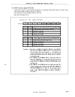
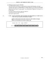
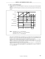
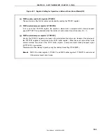
Figure 6-4. Register Setting for Interval Timer Mode Operation (2/2)
(c) TMP0 I/O control register 0 (TP0IOC0)
0
0
0
0
0/1
TP0IOC0
0: Disable TOP00 pin output
1: Enable TOP00 pin output
Setting of output level with
operation of TOP00 pin disabled
0: Low level
1: High level
0: Disable TOP01 pin output
1: Enable TOP01 pin output
Setting of output level with
operation of TOP01 pin disabled
0: Low level
1: High level
0/1
0/1
0/1
TP0OE1
TP0OL0
TP0OE0
TP0OL1
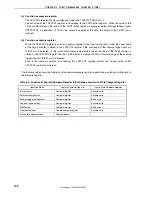
(d) TMP0 counter read buffer register (TP0CNT)
By reading the TP0CNT register, the count value of the 16-bit counter can be read.
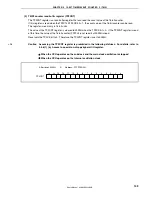
(e) TMP0 capture/compare register 0 (TP0CCR0)
If the TP0CCR0 register is set to D
0
, the interval is as follows.
Interval = (D
0
+ 1)
×
Count clock cycle
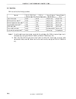
(f) TMP0
capture/compare
register 1 (TP0CCR1)
Usually, the TP0CCR1 register is not used in the interval timer mode. However, the set value of the
TP0CCR1 register is transferred to the CCR1 buffer register. A compare match interrupt request signal
(INTTP0CC1) is generated when the count value of the 16-bit counter matches the value of the CCR1
buffer register.
Therefore, mask the interrupt request by using the corresponding interrupt mask flag (TP0CCMK1).
Remark
TMP0 I/O control register 1 (TP0IOC1), TMP0 I/O control register 2 (TP0IOC2), and TMP0
option register 0 (TP0OPT0) are usually not used in the interval timer mode.
However, set the TP0IOC2 register to use the external event count input.

