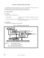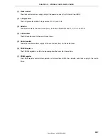
CHAPTER 9 8-BIT TIMER H
User’s Manual U16896EJ2V0UD
333
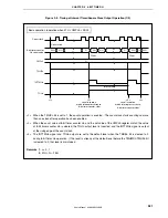
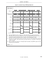
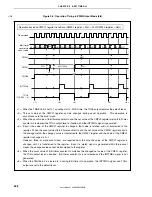
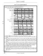
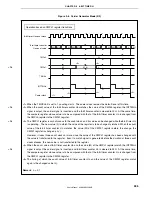
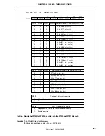
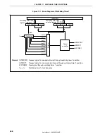
Figure 9-8. Carrier Generator Mode (1/3)
Operation when CMPn0 register = N, CMPn1 register = N is set
CMPn0
CMPn1
TMHEn
INTTMHn
Carrier clock
00H
N
00H
N
00H
N
00H
N
00H
N
00H
N
N
N
8-bit timer 5n count clock
TM5n count value
TCE5n
TOHn
0
0
1
1
0
0
1
1
0
0
INTTM5n
NRZBn
NRZn
Carrier clock
00H 01H
K
00H 01H
L
00H 01H
M 00H 01H
00H 01H
N
INTTM5Hn
<1> <2>
<3>
<4>
<5>
<6>
K
L
M
N
<6>
<7>
8-bit timer Hn count clock
8-bit timer counter
Hn count value
CR5n
<1> When the TMHEn bit = 0 and the TCE5n bit = 0, the operation of 8-bit timer Hn is stopped.
<2> When the TMHEn bit is set to 1, 8-bit timer Hn starts counting. The carrier clock remains the default level.
<3>
When the count value of 8-bit timer counter Hn and the set value of the CMPn0 register match, the first
INTTMHn signal is generated, the carrier clock signal is inverted, and the register that is compared with 8-bit
timer counter Hn changes from the CMPn0 register to the CMPn1 register. 8-bit timer counter Hn is cleared
to 00H.
<4> When the count value of 8-bit timer counter Hn and the set value of the CMPn1 register match, the INTTMHn
signal is generated, the carrier clock signal is inverted, and the register that is compared with 8-bit timer
counter Hn changes from the CMPn1 register to the CMPn0 register. 8-bit timer counter Hn is cleared to 00H.
A carrier clock with a duty of 50% is generated through the repetition of steps <3> and <4>.
<5> The INTTM5n signal is synchronized with 8-bit timer Hn and output as the INTTM5Hn signal.
<6> The INTTM5Hn signal becomes the data transfer signal of the NRZBn bit, and the value of the NRZBn bit is
transferred to the NRZn bit.
<7> The TOHn output is made low level by clearing the NRZn bit = 0.
Remark
n = 0, 1
<R>
<R>

