


CHAPTER 15 CLOCKED SERIAL INTERFACE 0 (CSI0)
User’s Manual U16896EJ2V0UD
458
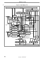
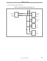
15.5 Output Pins
The following describes the output pins. For the setting of each pin, refer to
Table 4-12 Settings When Port Pins
Are Used for Alternate Functions
.
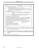
(1) SCK0n pin
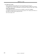
When the CSI0n operation is disabled (CSIM0n.CSI0En bit = 0), the SCK0n pin output status is as follows.
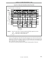
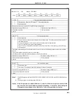
Table 15-2. SCK0n Pin Output Status
CKPn CKS0n2 CKS0n1 CKS0n0
SCK0n
Pin
Output
0
Don’t care
Don’t care
Don’t care
Fixed to high level
1 1 1
High
impedance
1
Other than above
Fixed to low level
Remark
n = 0, 1
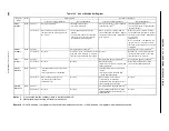
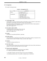
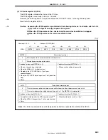
(2) SO0n pin
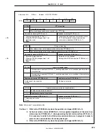
When the CSI0n operation is disabled (CSI0En bit = 0), the SO0n pin output status is as follows.
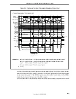
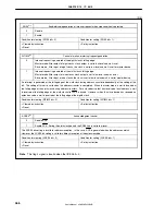
Table 15-3. SO0n Pin Output Status
TRMDn
DAPn
AUTOn
CCLn
DIRn
SO0n Pin Output
0
Don’t care
Don’t care
Don’t care
Don’t care
Fixed to low level
0
Don’t care
Don’t care
Don’t care
SO latch value (low level)
0 SOTBn7
bit
value
0
1 SOTBn0
bit
value
0
SOTBn15 bit value
0
1
1 SOTBn0
bit
value
0
SOTBFn7 bit value
0
1
SOTBFn0 bit value
0
SOTBFn15 bit value
1
1
1
1
1
SOTBFn0 bit value
Remark
n = 0, 1


