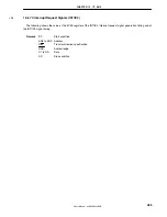
CHAPTER 16 I
2
C BUS
User’s Manual U16896EJ2V0UD
475
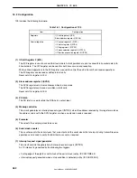
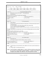
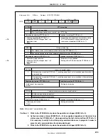
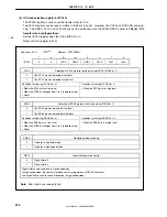
(5) IIC function expansion register 0 (IICX0)
This register sets the function expansion of I
2
C0 (valid only in high-speed mode).
This register can be read or written in 8-bit or 1-bit units. The CLX0 bit is set in combination with the
IICCL0.SMC0, IICCL0.CL01, and IICCL0.CL00 bits (refer to
16.3 (6) I
2
C0 transfer clock setting method
).
Set the IICX0 register when the IICC0.IICE0 bit = 0.
Reset sets this register to 00H.
After reset: 00H
R/W
Address: FFFFFD85H
7 6 5 4 3 2 1
<0>
IICX0
0 0 0 0 0 0 0
CLX0
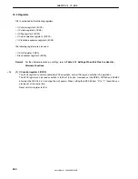
(6) I
2
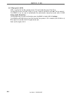
C0 transfer clock setting method
The I
2
C0 transfer clock frequency (f
SCL
) is calculated using the following expression.
f
SCL
= 1/(m
×
T + t
R
+ t
F
)
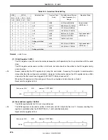
m = 12, 24, 48, 54, 86, 88, 172, 198 (refer to
Table 16-2 Selection Clock Setting
)
T: 1/f
XX
t
R
:
SCL0 rise time
t
F
:
SCL0 fall time
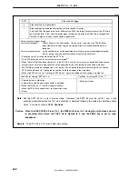
For example, the I
2
C0 transfer clock frequency (f
SCL
) when f
XX
= 20 MHz, m = 54, t
R
= 200 ns, and t
F
= 50 ns is
calculated using following expression.
f
SCL
= 1/(54
×
50 ns + 200 ns + 50 ns)
≅
339 kHz
m
×
T + t
R
+ t
F
m/2
×
T
t
F
t
R
m/2
×
T
SCL0
SCL0 inversion
SCL0 inversion
SCL0 inversion
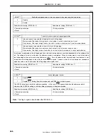
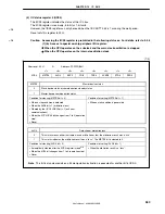
The selection clock is set using a combination of the IICCL0.SMC0, IICCL0.CL01, and IICCL0.CL00 bits and the
IICX0.CLX0 bit.
<R>

