CHAPTER 13 A/D CONVERTER
User’s Manual U16896EJ2V0UD
386
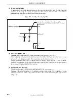
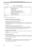
(4) Measures against noise
To keep a resolution of 10 bits, be aware of noise on the AV
REF0
and ANI0 to ANI7 pins. The higher the output
impedance of the analog input source, the greater the effect of noise. Therefore, it is recommended to
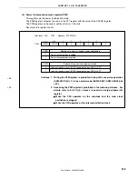
connect external capacitors as shown in Figure 13-8 to reduce noise.
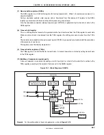
Figure 13-8. Handling of Analog Input Pins
AV
REF0
ANI0 to ANI7
AV
SS
V
SS
If noise of AV
REF0
or higher or AV
SS
or lower could be
generated, clamp with a diode with a small V
F
(0.3 V or lower).
Reference voltage input
C
≥
0.1 F
μ
(5) ANI0/P70 to ANI7/P77 pins
The analog input pins (ANI0 to ANI7) function alternately as input port pins (P70 to P77).
When performing A/D conversion by selecting any of the ANI0 to ANI7 pins, do not execute an input
instruction to port 7 during conversion. This may decrease the conversion resolution.
If digital pulses are applied to the pin adjacent to the pin subject to A/D conversion, the value of the A/D
conversion may differ from the expected value because of coupling noise. Therefore, do not apply pulses to
the pin adjacent to the pin subject to A/D conversion.
(6) Input impedance of AV
REF0
pin
A series resistor string of tens of k
Ω
is connected between the AV
REF0
pin and AV
SS
pin.
Therefore, if the output impedance of the reference voltage source is high, this will result in a series
connection to the series resistor string between the AV
REF0
pin and AV
SS
pin, resulting in a large reference
voltage error.

