

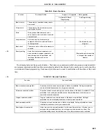
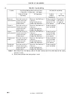
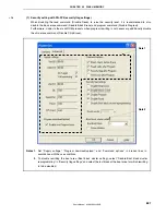


CHAPTER 26 FLASH MEMORY
User’s Manual U16896EJ2V0UD
637
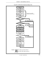
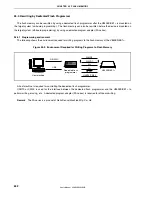
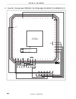
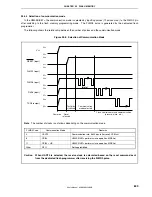
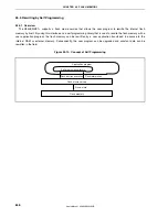
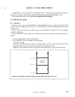
Figure 26-6. Wiring Example of V850ES/KE1+ Flash Writing Adapter (FA-64GK-9ET-A, FA-64GB-8EU-A) (2/2)
Notes 1.
Wire the FLMD1 pin as shown in the figure, or connect it to GND on board via a pull-down resistor.
2.
The above figure shows an example of wiring when the clock is supplied from the PG-FP4.
Be sure to set and connect as follows when the clock is supplied from the PG-FP4.
•
Set J1 of the flash adapter (FA) to the VDD side.
•
Connect CLKOUT of FA to CLKIN of FA.
•
Connect X1 of FA to X1 of the device.
•
Connect X2 of FA to X2 of the device.
If an oscillator is created on the flash adapter and a clock is supplied, the above setting and
connections will not necessary. The following shows a circuit example.
X1
X2
3.
Corresponding pin when using UART0
Remarks 1.
Handle the pins not described above in accordance with the specified handling of unused pins
(refer to
2.2 Pin I/O Circuits and Recommended Connection of Unused Pins)
.
When connecting to V
DD
via a resistor, use of a resistor of 1 k
Ω
to 10 k
Ω
is recommended.
2.
This adapter is for a 64-pin plastic LQFP (fine pitch) package.
3.
This diagram shows the wiring when using a handshake-supporting CSI.
<R>


