CHAPTER 3 CPU FUNCTIONS
User’s Manual U16896EJ2V0UD
55
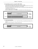
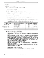
(3) On-chip peripheral I/O area
A 4 KB area from 3FFF000H to 3FFFFFFH is reserved as the on-chip peripheral I/O area.
Figure 3-6. On-Chip Peripheral I/O Area
3FFFFFFH
3FFF000H
On-chip peripheral I/O area
(4 KB)
FFFFFFFH
FFFF000H
Physical address space
Logical address space
Peripheral I/O registers assigned with functions such as on-chip peripheral I/O operation mode specification
and state monitoring are mapped to the on-chip peripheral I/O area. Program fetches are not allowed in this
area.
Cautions 1. If word access of a register is attempted, halfword access to the word area is performed
twice, first for the lower bits, then for the higher bits, ignoring the lower 2 address bits.
2. If a register that can be accessed in byte units is accessed in halfword units, the higher 8
bits become undefined if the access is a read operation. If a write access is performed,
only the data in the lower 8 bits is written to the register.
3. Addresses that are not defined as registers are reserved for future expansion. If these
addresses are accessed, the operation is undefined and not guaranteed.
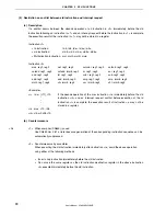
(4) Number of clocks for access
The following table shows the number of base clocks required for accessing each resource.
Area (Bus Width)
Bus Cycle Type
Internal ROM
(32 Bits)
Internal RAM
(32 Bits)
On-Chip Peripheral I/O
(16 Bits)
Instruction fetch (normal access)
1
1
Note 1
−
Instruction fetch (branch)
2
2
Note 1
−
Operand data access
3
1
3
Note 2
Notes 1.
If the access conflicts with a data access, the number of clock is incremented by 1.
2.
This value varies depending on the setting of the VSWC register.
Remark
Unit:
Clocks/access

