


CHAPTER 13 A/D CONVERTER
User’s Manual U16896EJ2V0UD
385
13.6 Cautions
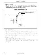
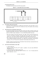
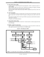
(1) Power
consumption in standby mode
The operation of the A/D converter stops in the standby mode. At this time, the power consumption can be
reduced by stopping the conversion operation (the ADM.ADCS bit = 0) and stopping the reference voltage
circuit (ADM.ADCS2 bit = 0).
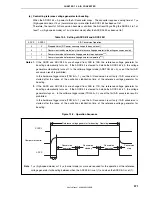
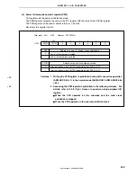
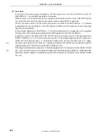
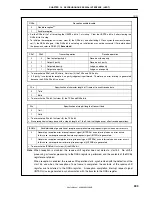
Figure 13-7 shows an example of how to reduce the power consumption in the standby mode.
Figure 13-7. Example of How to Reduce Power Consumption in Standby Mode
ADCS
ADCS2
Series resistor string
AV
REF0
P-ch
AV
SS
Reference voltage circuit
(2) Input range of ANI0 to ANI7 pins
Use the A/D converter with the ANI0 to ANI7 pin input voltages within the specified range. If a voltage of
AV
REF0
or higher or AV
SS
or lower (even if within the absolute maximum ratings) is input to these pins, the
conversion value of the channel is undefined. Also, this may affect the conversion value of other channels.
(3) Conflicting
operations
(a) Conflict between writing to the ADCR register and reading from ADCR register upon the end of
conversion
Reading the ADCR register takes precedence. After the register has been read, a new conversion result
is written to the ADCR register.
(b) Conflict between writing to the ADCR register and writing to the ADM register or writing to the ADS
register upon the end of conversion
Writing to the ADM register or ADS register takes precedence. The ADCR register is not written, and
neither is the conversion end interrupt request signal (INTAD) generated.
<R>


