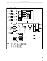
CHAPTER 1 INTRODUCTION
User’s Manual U16896EJ2V0UD
26
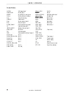
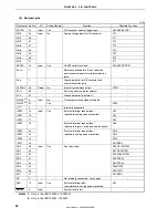
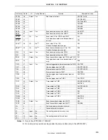
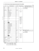
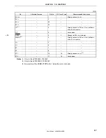
Pin identification
ADTRG:
A/D trigger input
ANI0 to ANI7:
Analog input
ASCK0: Asynchronous
serial
clock
AV
REF0
:
Analog reference voltage
AV
SS
:
Ground for analog
CLKOUT: Clock
output
EV
DD
:
Power supply for port
EV
SS
:
Ground for port
FLMD0, FLMD1:
Flash programming mode
IC: Internally
connected
INTP0 to INTP7:
External interrupt input
KR0 to KR7:
Key return
NC: Non-connection
NMI: Non-maskable
interrupt
request
P00 to P06:
Port 0
P30 to P35, P38, P39: Port 3
P40 to P42:
Port 4
P50 to P55:
Port 5
P70 to P77:
Port 7
P90, P91, P96 to P99,
P913 to P915:
Port 9
PCM0, PCM1:
Port CM
PDL0 to PDL7:
Port DL
RESET: Reset
RTP00 to RTP05:
Real-time output port
RXD0, RXD1:
Receive data
SCK00, SCK01:
Serial clock
SCL0: Serial
clock
SDA0: Serial
data
SI00, SI01:
Serial input
SO00, SO01:
Serial output
TI010, TI011,
TI50, TI51,
TIP00, TIP01:
Timer input
TO01,
TO50, TO51,
TOH0, TOH1,
TOP00, TOP01:
Timer output
TXD0, TXD1:
Transmit data
V
DD
: Power
supply
V
SS
: Ground
X1, X2:
Crystal for main clock
XT1, XT2:
Crystal for subclock

