

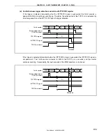
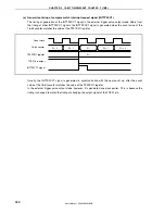
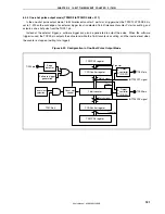


CHAPTER 6 16-BIT TIMER/EVENT COUNTER P (TMP)
User’s Manual U16896EJ2V0UD
182
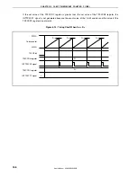
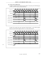
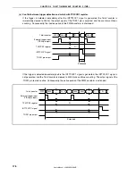
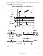
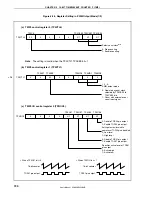
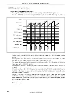
Figure 6-21. Basic Timing in One-Shot Pulse Output Mode
FFFFH
16-bit counter
0000H
TP0CE bit
TP0CCR0 register
INTTP0CC0 signal
TP0CCR1 register
INTTP0CC1 signal
TOP01 pin output
External trigger input
(TIP00 pin input)
D
1
D
0
D
0
D
1
D
1
D
1
D
0
D
0
Delay
(D
1
)
Active
level width
(D
0
−
D
1
+ 1)
Delay
(D
1
)
Active
level width
(D
0
−
D
1
+ 1)
Delay
(D
1
)
Active
level width
(D
0
−
D
1
+ 1)
TOP00 pin output
(software trigger)
When the TP0CE bit is set to 1, 16-bit timer/event counter P waits for a trigger. When the trigger is generated, the
16-bit counter is cleared from FFFFH to 0000H, starts counting, and outputs a one-shot pulse from the TOP01 pin.
After the one-shot pulse is output, the 16-bit counter is set to FFFFH, stops counting, and waits for a trigger. If a
trigger is generated again while the one-shot pulse is being output, it is ignored.
The output delay period and active level width of the one-shot pulse can be calculated as follows.
Output delay period = (Set value of TP0CCR1 register)
×
Count clock cycle
Active level width = (Set value of TP0CCR0 register
−
Set value of TP0CCR1 re 1)
×
Count clock cycle
The compare match interrupt request signal INTTP0CC0 is generated when the 16-bit counter counts after its
count value matches the value of the CCR0 buffer register. The compare match interrupt request signal INTTP0CC1
is generated when the count value of the 16-bit counter matches the value of the CCR1 buffer register.
The valid edge of an external trigger input or setting the software trigger (TP0CTL1.TP0EST bit) to 1 is used as the
trigger.


