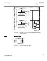
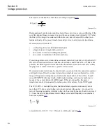
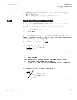

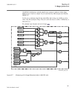
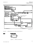

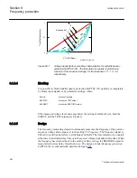

8.4.2.6
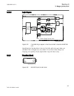
Logic diagram
ANSI05000162-2-en.vsd
OR
&
&
BLOCK
Xleakage
Ei
M=
(Ei / f)
(Vn / fn)
M = relative Pickup as service value
Pickup2
M>Pickup2
Pickup1
M>Pickup1
IEEE law
Tailor-made law
Calculation
of internal
induced
voltage Ei
TD
M
M
M
ALARM
TRIP
AlarmPickup
0
0
0-tMax
0
0-tMax
0-tMax
t>tAlarm
t>tMin
t_MaxTripDelay
t_MinTripDelay
tAlarm
V3P
I3P
ANSI05000162 V2 EN
Figure 275:
A simplified logic diagram of the Overexcitation protection OEXPVPH
(24)
Simplification of the diagram is in the way the IEEE and Tailor-made delays are
calculated. The cooling process is not shown. It is not shown that voltage and
frequency are separately checked against their respective limit values.
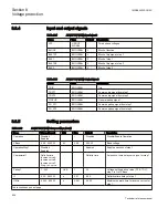
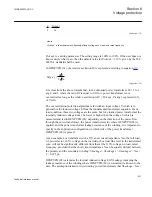
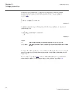
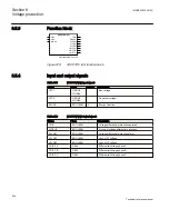
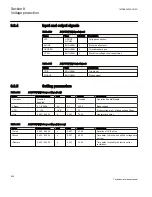
8.4.3
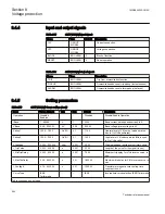
Function block
ANSI05000329-2-en.vsd
OEXPVPH (24)
I3P*
V3P*
BLOCK
RESET
TRIP
PICKUP
ALARM
ANSI05000329 V2 EN
Figure 276:
OEXPVPH (24) function block
1MRK505222-UUS C
Section 8
Voltage protection
539
Technical reference manual
Summary of Contents for Relion 670 series
Page 1: ...Relion 670 series Line differential protection RED670 ANSI Technical reference manual...
Page 2: ......
Page 40: ...34...
Page 50: ...44...
Page 60: ...54...
Page 126: ...120...
Page 384: ...378...
Page 496: ...490...
Page 556: ...550...
Page 602: ...596...
Page 620: ...614...
Page 794: ...788...
Page 864: ...858...
Page 988: ...982...
Page 998: ...992...
Page 1084: ...1078...
Page 1164: ...1158...
Page 1168: ...1162...
Page 1220: ...1214...
Page 1230: ...1224...
Page 1231: ...1225...