3 General Safety Precautions and Usage Considerations
3-12
(1) Lead insertion hole intervals on the printed circuit board should match the lead pitch of the device
precisely.
(2) If lead insertion hole intervals on the printed circuit board do not precisely match the lead pitch of the
device, do not attempt to forcibly insert devices by pressing on them or by pulling on their leads.
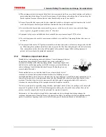
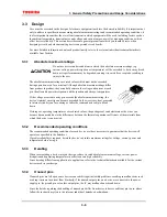
(3) For the minimum clearance specification between a device and a printed
circuit board, refer to the relevant device’s datasheet and databook. If
necessary, achieve the required clearance by forming the device’s leads
appropriately. Do not use the spacers which are used to raise devices above
the surface of the printed circuit board during soldering to achieve clearance.
These spacers normally continue to expand due to heat, even after the solder
has begun to solidify; this applies severe stress to the device.
(4) Observe the following precautions when forming the leads of a device prior to mounting.
•
Use a tool or jig to secure the lead at its base (where the lead meets the device package) while bending so as
to avoid mechanical stress to the device. Also avoid bending or stretching device leads repeatedly.
•
Be careful not to damage the lead during lead forming.
•
Follow any other precautions described in the individual datasheets and databooks for each device and
package type.
3.5.2 Socket
mounting
(1) When socket mounting devices on a printed circuit board, use sockets which match the inserted device’s
package.
(2) Use sockets whose contacts have the appropriate contact pressure. If the contact pressure is insufficient, the
socket may not make a perfect contact when the device is repeatedly inserted and removed; if the pressure
is excessively high, the device leads may be bent or damaged when they are inserted into or removed from
the socket.
(3) When soldering sockets to the printed circuit board, use sockets whose construction prevents flux from
penetrating into the contacts or which allows flux to be completely cleaned off.
(4) Make sure the coating agent applied to the printed circuit board for moisture-proofing purposes does not
stick to the socket contacts.
(5) If the device leads are severely bent by a socket as it is inserted or removed and you wish to repair the leads
so as to continue using the device, make sure that this lead correction is only performed once. Do not use
devices whose leads have been corrected more than once.
(6) If the printed circuit board with the devices mounted on it will be subjected to vibration from external
sources, use sockets which have a strong contact pressure so as to prevent the sockets and devices from
vibrating relative to one another.
3.5.3 Soldering
temperature
profile
The soldering temperature and heating time vary from device to device. Therefore, when specifying the
mounting conditions, refer to the individual datasheets and databooks for the devices used.
(1) Using a soldering iron
Complete soldering within ten seconds for lead temperatures of up to 260°C, or within three seconds for lead
temperatures of up to 350°C.
Содержание TMPR4925
Страница 1: ...64 Bit TX System RISC TX49 Family TMPR4925 Rev 3 0 ...
Страница 4: ......
Страница 15: ...Handling Precautions ...
Страница 16: ......
Страница 18: ...1 Using Toshiba Semiconductors Safely 1 2 ...
Страница 40: ...3 General Safety Precautions and Usage Considerations 3 18 ...
Страница 42: ...4 Precautions and Usage Considerations 4 2 ...
Страница 43: ...TMPR4925 ...
Страница 44: ......
Страница 54: ...Chapter 1 Features 1 8 ...
Страница 58: ...Chapter 2 Block Diagram 2 4 ...
Страница 88: ...Chapter 4 Address Mapping 4 12 ...
Страница 226: ...Chapter 8 DMA Controller 8 58 ...
Страница 260: ...Chapter 9 SDRAM Controller 9 34 ...
Страница 480: ...Chapter 15 Interrupt Controller 15 32 ...
Страница 554: ...Chapter 19 Real Time Clock RTC 19 8 ...
Страница 555: ...Chapter 20 Removed 20 1 20 Removed ...
Страница 556: ...Chapter 20 Removed 20 2 ...
Страница 564: ...Chapter 21 Extended EJTAG Interface 21 8 ...
Страница 580: ...Chapter 22 Electrical Characteristics 22 16 ...
Страница 586: ...Chapter 23 Pin Layout Package 23 6 23 2 Package Package Type Package Code 256 pin PBGA PBGA 4L P BGA256 2727 1 27A4 ...
Страница 588: ...Chapter 24 Usage Notes 24 2 ...
Страница 590: ...Appendix A TX49 H2 Core Supplement A 2 ...

