Chapter 14 AC-link Controller
14-9
14.3.6 Sample-data Transmission and Reception
This section describes the mechanism for transmission and reception of PCM audio and modem
wave-data. An overview is described first. The DMA (Direct Memory Access) operation, error
detection and recovery procedure follow. A special case using slot activation control is described last.
14.3.6.1 Overview
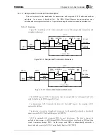
Figure 14.3.6 and Figure 14.3.7 show conceptual views of the sample-data transmission and
reception mechanisms.
Figure 14.3.6 Sample-data Transmission Mechanism
Figure 14.3.7 Sample-data Reception Mechanism
The CODEC requests ACLC to transmit and receive sample-data via ‘slot-request’ and ‘slot-
valid’ bit-fields on the SDIN signal of AC-link.
For transmission, ACLC transmits the data with ‘slot-valid’ tag set. For reception, ACLC
captures the slot-data.
Transmission or reception through each stream can be independently activated or deactivated
under control of ACLC Slot Enable Register (ACSLTEN).
ACLC is equipped with a separate FIFO for each data-stream. The data to transmit is
prefetched from memory to FIFO through DMA. The received data is buffered on FIFO and then
stored to memory through DMA. In this stage, each DMA is independently activated or
deactivated under control of ACLC Control Enable Register (ACCTLEN).
DMAC
FIFO
DMA
Buffer
Memory
Read
Data
DMAREQ
Write
Data
ACCTLEN
REQ
Latch
Strobe
ACSLTEN
Valid Flag
Data
Link-
side
Slot Req
Slot Valid,
Slot Data
AC-link
Underrun Error
ACLC
DMAC
FIFO
DMA
Buffer
Memory
Write
Data
DMAREQ
Read
Data
ACCTLEN
REQ
Latch
Strobe
ACSLTEN
Data
Link-
side
Slot Valid,
Slot Data
AC-link
Overrun Error
ACLC
Содержание TMPR4925
Страница 1: ...64 Bit TX System RISC TX49 Family TMPR4925 Rev 3 0 ...
Страница 4: ......
Страница 15: ...Handling Precautions ...
Страница 16: ......
Страница 18: ...1 Using Toshiba Semiconductors Safely 1 2 ...
Страница 40: ...3 General Safety Precautions and Usage Considerations 3 18 ...
Страница 42: ...4 Precautions and Usage Considerations 4 2 ...
Страница 43: ...TMPR4925 ...
Страница 44: ......
Страница 54: ...Chapter 1 Features 1 8 ...
Страница 58: ...Chapter 2 Block Diagram 2 4 ...
Страница 88: ...Chapter 4 Address Mapping 4 12 ...
Страница 226: ...Chapter 8 DMA Controller 8 58 ...
Страница 260: ...Chapter 9 SDRAM Controller 9 34 ...
Страница 480: ...Chapter 15 Interrupt Controller 15 32 ...
Страница 554: ...Chapter 19 Real Time Clock RTC 19 8 ...
Страница 555: ...Chapter 20 Removed 20 1 20 Removed ...
Страница 556: ...Chapter 20 Removed 20 2 ...
Страница 564: ...Chapter 21 Extended EJTAG Interface 21 8 ...
Страница 580: ...Chapter 22 Electrical Characteristics 22 16 ...
Страница 586: ...Chapter 23 Pin Layout Package 23 6 23 2 Package Package Type Package Code 256 pin PBGA PBGA 4L P BGA256 2727 1 27A4 ...
Страница 588: ...Chapter 24 Usage Notes 24 2 ...
Страница 590: ...Appendix A TX49 H2 Core Supplement A 2 ...

