Chapter 16 CHI Module
16-24
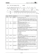
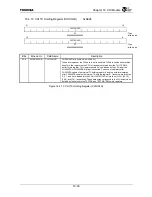
16.4.4 CHI Receive Pointer B Register (RXPTRB)
0xA80C
31 29
28 24
23 21
20 16
Reserved RXPTRB3 Reserved
RXPTRB2
W W
:
Type
00000 00000
:
Initial
value
15
13
12
8
7 5
4 0
Reserved RXPTRB1 Reserved
RXPTRB0
W W
:
Type
00000 00000
:
Initial
value
Bits Mnemonic Field
Name
Description
31:29
⎯
Reserved
⎯
28:24
RXPTRB3[4:0]
CHIRXPTRB3
CHIRXPTRB3 bits (Initial value: 00000, W)
These bits represent the TDM switch pointer which defines the receive channel
timeslot for byte 3 of the CHI receive holding register B; register B handles all
timeslots from channel (CHINCHAN
+
1) to channel (CHINCHAN
×
2
+
1). The
value loaded for this TDM switch pointer is the desired timeslot number minus
(CHINCHAN
+
1).
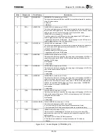
23:21
⎯
Reserved
⎯
20:16
RXPTRB2[4:0]
CHIRXPTRB2
CHIRXPTRB2 bits (Initial value: 00000, W)
These bits represent the TDM switch pointer which defines the receive channel
timeslot for byte 2 of the CHI receive holding register B; register B handles all
timeslots from channel (CHINCHAN
+
1) to channel (CHINCHAN
×
2
+
1). The
value loaded for this TDM switch pointer is the desired timeslot number minus
(CHINCHAN
+
1).
15:13
⎯
Reserved
⎯
12:8
RXPTRB1[4:0]
CHIRXPTRB1
CHIRXPTRB1 bits (Initial value: 00000, W)
These bits represent the TDM switch pointer which defines the receive channel
timeslot for byte 1 of the CHI receive holding register B; register B handles all
timeslots from channel (CHINCHAN
+
1) to channel (CHINCHAN
×
2
+
1). The
value loaded for this TDM switch pointer is the desired timeslot number minus
(CHINCHAN
+
1).
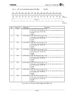
7:5
⎯
Reserved
⎯
4:0
RXPTRB0[4:0]
CHIRXPTRB0
CHIRXPTRB0 bits (Initial value: 00000, W)
These bits represent the TDM switch pointer which defines the receive channel
timeslot for byte 0 of the CHI receive holding register B; register B handles all
timeslots from channel (CHINCHAN
+
1) to channel (CHINCHAN
×
2
+
1). The
value loaded for this TDM switch pointer is the desired timeslot number minus
(CHINCHAN
+
1).
Figure 16.4.4 CHI Receive Pointer B Register (RXPTRB)
Содержание TMPR4925
Страница 1: ...64 Bit TX System RISC TX49 Family TMPR4925 Rev 3 0 ...
Страница 4: ......
Страница 15: ...Handling Precautions ...
Страница 16: ......
Страница 18: ...1 Using Toshiba Semiconductors Safely 1 2 ...
Страница 40: ...3 General Safety Precautions and Usage Considerations 3 18 ...
Страница 42: ...4 Precautions and Usage Considerations 4 2 ...
Страница 43: ...TMPR4925 ...
Страница 44: ......
Страница 54: ...Chapter 1 Features 1 8 ...
Страница 58: ...Chapter 2 Block Diagram 2 4 ...
Страница 88: ...Chapter 4 Address Mapping 4 12 ...
Страница 226: ...Chapter 8 DMA Controller 8 58 ...
Страница 260: ...Chapter 9 SDRAM Controller 9 34 ...
Страница 480: ...Chapter 15 Interrupt Controller 15 32 ...
Страница 554: ...Chapter 19 Real Time Clock RTC 19 8 ...
Страница 555: ...Chapter 20 Removed 20 1 20 Removed ...
Страница 556: ...Chapter 20 Removed 20 2 ...
Страница 564: ...Chapter 21 Extended EJTAG Interface 21 8 ...
Страница 580: ...Chapter 22 Electrical Characteristics 22 16 ...
Страница 586: ...Chapter 23 Pin Layout Package 23 6 23 2 Package Package Type Package Code 256 pin PBGA PBGA 4L P BGA256 2727 1 27A4 ...
Страница 588: ...Chapter 24 Usage Notes 24 2 ...
Страница 590: ...Appendix A TX49 H2 Core Supplement A 2 ...


