Chapter 16 CHI Module
16-4
16.3.2 Receiver
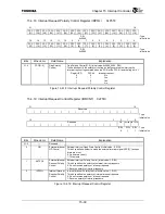
For the CHI receive direction, Buffer-A and Buffer-B receive holding registers are read either by the
DMA circuit or directly by the CPU. Each of these 2 holding registers are 32 bits wide, and CHI control
logic determines which byte to which holding register gets loaded at a given time from the 8-bit receive
shift register. In addition, the byte data loaded from the shift register to the holding register can be
MSB-first or LSB-first. Similar to the transmit direction, the receive section also operates in a ping-
pong fashion, allowing one buffer to be read (via the DMA or CPU) while the other buffer is being
loaded from the shift register a byte at a time, depending on which timeslots are active.
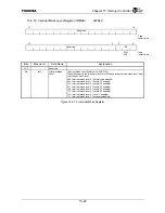
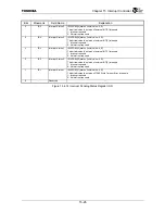
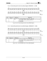
The receive TDM switch control register (independent from the transmit TDM switch control
register) is used to select ANY 4 channels per buffer to be loaded from the shift register to the holding
register. Each of the 8 selected channels also has an individual control bit for enabling/disabling the
timeslot.
An interrupt is available whenever a valid 32 bit word is available from the receive data holding
register A. This also means a valid CHI output sample can be written to the transmit data holding
register A. Similarly, an interrupt is also available whenever a valid 32 bit word is available from the
receive data holding register B. This also means a valid CHI output sample can be written to the
transmit data holding register B.
16.3.3 Clock and Control Generation
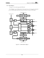
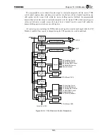
The CHI Module contains several programmable counters which are used to generate the various
CHI internal and external control signals and clocks. See Figure 16.3.2 for a block diagram of the CHI
clock and control generation circuit. As mentioned previously, CHICLK can be configured as either an
output (master mode) or input (slave mode). As an output, CHICLK is derived by dividing down from
IMBUSCLKF. In this mode, all CHI clocks are then synchronously locked to the main TX4925 system
clock. As an input, CHICLK is generated from an external clock source, which is asynchronous with
respect to IMBUSCLKF. The TX4925 CHI Module utilizes a digital-PLL circuit to stay “locked” to the
external source, while still operating internally using IMBUSCLKF CHIDIN and CHIDOUT are also
synchronized between IMBUSCLKF and the externally-supplied CHICLK.
CHIFS can also be configured as either an output (master mode) or input (slave mode). As an output,
CHIFS is derived by dividing down from CHICLK. For this mode, the CHIFS pulse width and polarity
is also programmable. As an input, CHIFS is generated from an external sync source. The TX4925 CHI
Module utilizes a digital-PLL circuit to stay “locked” to the external sync source, while still operating
internally using IMBUSCLKF.
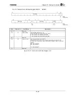
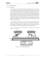
The programmable receive and transmit sync delay counters shown in See Figure 16.3.2 are used to
implement the bit offset feature described earlier. The bit offset control bits determine the number of
clock cycles between the start of timeslot 0 and CHIFS. The receive and transmit sync delay counters
are independent from each other, such that the receive and transmit serial data streams can have
different bit offsets.
Содержание TMPR4925
Страница 1: ...64 Bit TX System RISC TX49 Family TMPR4925 Rev 3 0 ...
Страница 4: ......
Страница 15: ...Handling Precautions ...
Страница 16: ......
Страница 18: ...1 Using Toshiba Semiconductors Safely 1 2 ...
Страница 40: ...3 General Safety Precautions and Usage Considerations 3 18 ...
Страница 42: ...4 Precautions and Usage Considerations 4 2 ...
Страница 43: ...TMPR4925 ...
Страница 44: ......
Страница 54: ...Chapter 1 Features 1 8 ...
Страница 58: ...Chapter 2 Block Diagram 2 4 ...
Страница 88: ...Chapter 4 Address Mapping 4 12 ...
Страница 226: ...Chapter 8 DMA Controller 8 58 ...
Страница 260: ...Chapter 9 SDRAM Controller 9 34 ...
Страница 480: ...Chapter 15 Interrupt Controller 15 32 ...
Страница 554: ...Chapter 19 Real Time Clock RTC 19 8 ...
Страница 555: ...Chapter 20 Removed 20 1 20 Removed ...
Страница 556: ...Chapter 20 Removed 20 2 ...
Страница 564: ...Chapter 21 Extended EJTAG Interface 21 8 ...
Страница 580: ...Chapter 22 Electrical Characteristics 22 16 ...
Страница 586: ...Chapter 23 Pin Layout Package 23 6 23 2 Package Package Type Package Code 256 pin PBGA PBGA 4L P BGA256 2727 1 27A4 ...
Страница 588: ...Chapter 24 Usage Notes 24 2 ...
Страница 590: ...Appendix A TX49 H2 Core Supplement A 2 ...

