Chapter 3 Signals
3-7
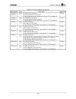
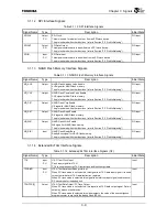
3.1.6
Serial I/O Interface Signals
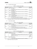
Table 3.1.6 Serial I/O Interface Signals
Signal Name
Type
Description
Initial State
CTS [1:0]
*
Input
PU
*
1
SIO Clear to Send
CTS
*
signals.
The pins are shared with other functions (refer to Section "3.3 Pin Multiplexing").
PIO input
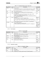
RTS [1:0]
*
Output
PU
*
1
SIO Request to Send
RTS
*
signals.
The pins are shared with other functions (refer to Section "3.3 Pin Multiplexing").
PIO input
RXD[1:0] Input
PU
*
1
SIO Receive Data
Serial data input signals.
The pins are shared with other functions (refer to Section "3.3 Pin Multiplexing").
PIO input
TXD[1:0]
3-state
Output
PU
*
1
SIO Transmit Data
Serial data output signals.
The pins are shared with other functions (refer to Section "3.3 Pin Multiplexing").
PIO input
SCLK Input
PU
External Serial Clock
SIO clock input signal. SIO0 and SIO1 share this signal.
The pin is shared with other functions (refer to Section "3.3 Pin Multiplexing").
PIO input
*
1:
These signals are pulled up for channel 0 only. No pull-up resistor is provided for channel 1.
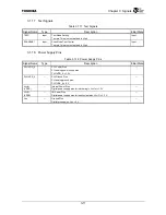
3.1.7 Timer
Interface
Signals
Table 3.1.7 Timer Interface Signals
Signal Name
Type
Description
Initial State
TIMER[1:0] Output
PU
Timer Output
Timer output signals.
The pins are shared with other functions (refer to Section "3.3 Pin Multiplexing").
PIO input
TCLK Input
PU
External Timer Clock
Timer input clock signal. TMR0, TMR1, and TMR2 share this signal.
The pin is shared with other functions (refer to Section "3.3 Pin Multiplexing").
PIO input
3.1.8
Parallel I/O Interface Signals
Table 3.1.8 Parallel I/O Interface Signals
Signal Name
Type
Description
Initial State
PIO[31:20] Input/output
PU
PIO Ports[31:20]
Parallel I/O signals.
The pins are shared with other functions, including PC trace (refer to Section "3.3 Pin
Multiplexing"). The boot configuration signal on the TDO pin determines whether the
signals are used for PC trace.
Selected by
TDO
H: PIO input
L: Output
(PC trace
function)
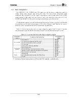
PIO[19:0] Input/output
PU
*
1
PIO Ports[19:0]
Parallel I/O signals.
The pins are shared with other functions (refer to Section "3.3 Pin Multiplexing").
Input
*
1:
PIO[17:12] do not have pull-up resistors.
Содержание TMPR4925
Страница 1: ...64 Bit TX System RISC TX49 Family TMPR4925 Rev 3 0 ...
Страница 4: ......
Страница 15: ...Handling Precautions ...
Страница 16: ......
Страница 18: ...1 Using Toshiba Semiconductors Safely 1 2 ...
Страница 40: ...3 General Safety Precautions and Usage Considerations 3 18 ...
Страница 42: ...4 Precautions and Usage Considerations 4 2 ...
Страница 43: ...TMPR4925 ...
Страница 44: ......
Страница 54: ...Chapter 1 Features 1 8 ...
Страница 58: ...Chapter 2 Block Diagram 2 4 ...
Страница 88: ...Chapter 4 Address Mapping 4 12 ...
Страница 226: ...Chapter 8 DMA Controller 8 58 ...
Страница 260: ...Chapter 9 SDRAM Controller 9 34 ...
Страница 480: ...Chapter 15 Interrupt Controller 15 32 ...
Страница 554: ...Chapter 19 Real Time Clock RTC 19 8 ...
Страница 555: ...Chapter 20 Removed 20 1 20 Removed ...
Страница 556: ...Chapter 20 Removed 20 2 ...
Страница 564: ...Chapter 21 Extended EJTAG Interface 21 8 ...
Страница 580: ...Chapter 22 Electrical Characteristics 22 16 ...
Страница 586: ...Chapter 23 Pin Layout Package 23 6 23 2 Package Package Type Package Code 256 pin PBGA PBGA 4L P BGA256 2727 1 27A4 ...
Страница 588: ...Chapter 24 Usage Notes 24 2 ...
Страница 590: ...Appendix A TX49 H2 Core Supplement A 2 ...


